Contents
- P-N Junction Diode
- Diode Function
- PN junction
- Forward bias
- Reverse bias
- Depletion layer-
- V-I Characteristics of Semiconductor P-N diode
- Knee voltage
- Breakdown voltage
- Doping
- Reverse Saturation Current
- • The Width of the Depletion Layer
- Barrier potential/built-in potential
- Application of p-n junction diode
- FAQ(frequently asked questions)
P-N Junction Diode
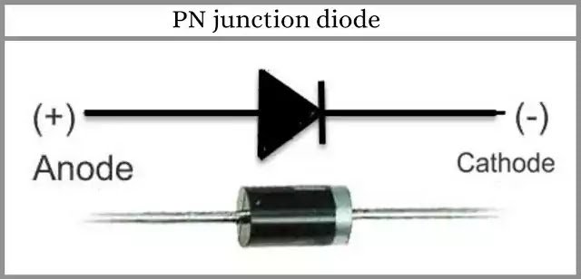
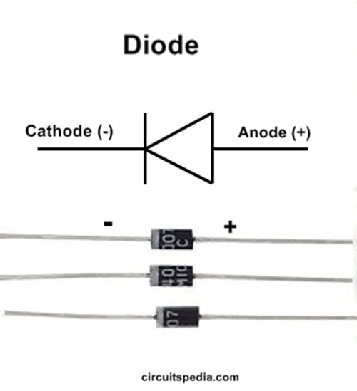
A diode is a two-terminal polarised electronic semiconductor device. One terminal is Anode(-) and the other is Cathode(+). The cathode is marked with a silver colour or colour band. This is the simplest semiconductor device but this is very important and most useful in electronic circuits.
Diode Function
The main function of the semiconductor diode is the flow of electrons to totally in only one direction across it. It means Diode conducts current in only one direction. so, this is a Unidirectional device. If change the polarity of the diode then no current passes through it. So we can say that diode acts as a switch that allows the conduction of current in only one direction. This is the property of an Ideal Diode.
- An ideal diode acts as a short circuit with the same polarity with supply, But in Reverse connection, it acts like Open circuit means no current flows in reverse polarity.
The semiconductor Diode is formed by adding and applying a burning force or crystallization on together of P-type and n-Type materials (p-n junction). Joining of Both materials should of the same base – Ge or Si. The PN-junction is the basic root for semiconductor diodes.
 PN junction
PN junction is made from a single piece of semiconductor of two different properties. One side is made to be P-type material, and the other side is made with N-type. Both ends of the PN-junction have different properties. One end has an excess/majority of electrons and the other end has an excess/majority of holes.
The p-type semiconductor is formed by adding trivalent impurities in pure or intrinsic semiconductor and the n-type semiconductor is formed by adding pentavalent impurities in a pure or intrinsic semiconductor.
P-type materials have majority charge carriers of holes and minority charge carriers of electrons. But in N-type materials have majority charge carriers of electrons and minority charge carriers of holes.
Half part of a-Si crystal is doped with a trivalent impurity and a half with pentavalent impurity, we get P-N junction diode. The border where p-type and n-region meet called the junction.
The free electrons move from the negative terminal (cathode) to the positive terminal (anode). But the current flow direction is from the positive terminal to the negative terminal.
Forward bias
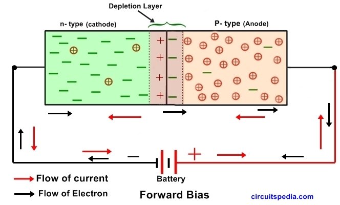
If the p-terminal of a diode is connected with a positive supply and the n-terminal is connected with a negative supply, then it is called forward bias. If the diode is forward-biased, it allows the electric current to flow. On the other hand, if the diode is reverse-biased, it blocks the electric current flow. In the Reverse bias mode, the PN diode works as a closed switch, and there is a flow of electric current through it.
Reverse bias
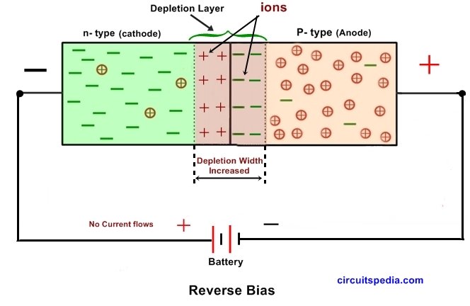
When the P- terminal of the diode is connected with the Negative terminal of the supply (Battery) and the N- terminal is connected with the Positive of the battery, this connection is called a Reverse bias connection. In this connection, no Electrons flow and no current flows. Reverse bias mode acts like an Open circuit means there is No Flow of current through it.
Depletion layer-
The depletion layer is created by the initial movement of the majority carrier across the junction. The hole concentration on p-type and electron concentration on n-type are very high. Due to the formation of the p-n junction by diffusion, electron moves from n-type to p-type, and holes move from p-type to n-type. The combination of electrons and holes at the junction creates ions, and there are only ions present at the junction. Ions are non-movable.
Therefore, when holes pass to electrons through these ions, then +ve ions repel the holes and oppose it passing to electrons, And created a resistance wall of very small width. This is called the Depletion layer. The width of depletion increases in reverse bias connection. Electric field intensity is created with the depletion layer. and the sign of this electric field is negative because the direction of the electric field is +ve to -ve.
• Depletion layer consists +ve charge and –ve charge on either side of junction.
• Depletion layer opposes only the majority carrier, not the minority carrier.
• The depletion layer is also called the Space charge region or transition region.
• Depletion layer consists of immobile charged particles.
V-I Characteristics of Semiconductor P-N diode
Knee voltage
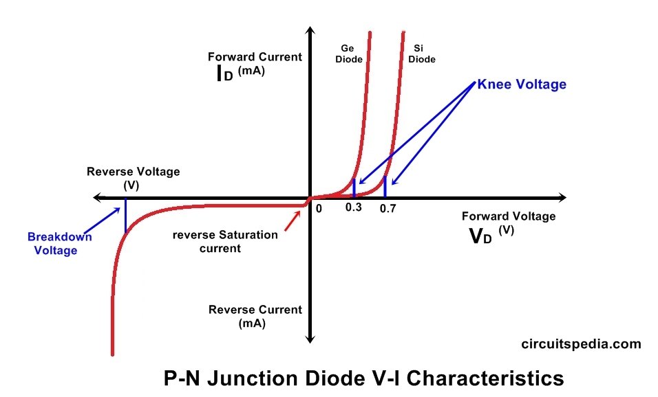
This is the minimum required voltage to start the conduction of current through the diode. This is also known as cut-in voltage. This is the forward voltage at which the diode current starts increasing rapidly.
The knee voltage of si diode is 0.7 voltage and the 0.3v of the Ge diode.
Breakdown voltage
This is the minimum amount of voltage of an insulator that makes it an electrical conductor.
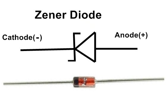
In Reverse bias connection of p-n diode. No, current flows through the diode, but when we increase the reverse voltage level continuously, the diode gets internal damage (breakdown) and starts conduction at a fixed level. Breakdown voltage is the Minimum Amount of reverse bias voltage at which the diode starts conduction in a reverse bias connection. This breakdown characteristics of the diode used in the Zener Diode which is always used in reverse bias and Limits the circuit voltage.
Doping
A material in pure form acts as an insulator. So making it more conductive in nature we need to add some impurities to it. The process of adding impurities in pure (intrinsic material) is called doping to change their electrical properties. Generally, trivalent and pentavalent elements are used to doping to a semiconductor. When a semiconductor is doped with a trivalent impurity(Boron, Aluminium), it becomes P-type semiconductor material. When dope any intrinsic material with Pentavalent impurity (phosphorus, arsenic, bismuth, antimony) then it becomes an N-type semiconductor.
Reverse Saturation Current
On both sides of the p-n junction, a very small amount of minority charge carrier is present. P-type minority charge carrier in the n-type side and n-type minority charge carrier on the p-type side. It also allows to flow a minority charge current. The current which is flowing by the minority carriers is called Reverse current.
When a voltage is applied on the junction, then further external reverse voltage flows due to minority charge carriers, and this increases external voltage but does not increase reverse current. At a voltage level where the current goes on a fixed maximum level and after, Only voltage increases and current does not increase. This is called reverse saturation current.
The reverse saturation current remains constant with the increase of voltage, But when voltage increases continuously then at a Level of voltage, the junction will get a breakdown and high reverse current will flow.
The reverse saturation current depends on temperature. If the temperature of the junction increases, the minority charge carriers also increase.
• The Width of the Depletion Layer
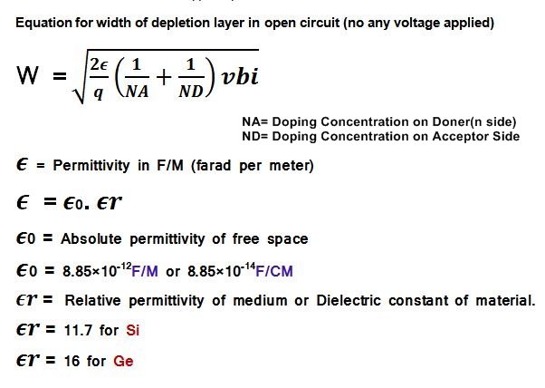
Practically The value of Depletion width varies from 0.1µm to 0.5µm
A typical value of Depletion width is -0.5µm
By increasing doping concentration Depletion layer width can be reduced
Electrons move across the PN junction from the N-type to the P-type, and they leave behind positively charged donor ions on the negative side. Holes from the acceptor impurity move across the junction in the opposite direction into the region where there are large numbers of free electrons.
As a result, the charge density of the P-type through the junction is filled with negatively charged acceptor ions, and the charge density of the N-type along with the junction becomes positive. This charge transfer of electrons and holes across the PN junction is known as diffusion.
Barrier potential/built-in potential
Simply Voltage formed across the depletion layer is called the contact potential. The built-in potential in a semiconductor equals the potential across the depletion region in thermal equilibrium. This is also called built-in potential or barrier voltage/potential or potential hill or diffusion voltage.
Contact potential always appears within the depletion layer It is noted as V0 or Vbi.
The contact potential of any diode can not measure by any instrument.
V0 for Ge diode = 0.1v to 0.5v typically we use V0=0.2v
V0 for Si diode = 0.6v to 0.9v typically V0= 0.7v
Application of p-n junction diode
• As Rectifier to convert AC to DC signal
• Clipper circuit for clipping the signal (changing the wave shape)
• To supply ( to protect from the reverse supply)
• Clamper circuit to restore the dc signal wave
• As Voltage multiplier
• In digital Logic circuit design
• In Demodulation Circuits
Other types of diode
Photodiode, Zener Diode, Gunn Diode, Tunnel Diode. PIN Diode, Varactor Diode. Light Emitting Diode (LED), Schottky Diode, Laser Diode, Switching Diode.
FAQ(frequently asked questions)
Q: What is a PN junction diode?
A: A PN junction diode is a two-terminal electronic device that is formed by joining together a P-type semiconductor region and an N-type semiconductor region. The junction between the P-type and N-type materials creates specific electrical characteristics.
Q: How does a PN junction diode work?
A: A PN junction diode works based on the principle of the P-N junction. When a forward bias voltage is applied across the diode (positive voltage at the P-side and negative voltage at the N-side), it allows current to flow easily through the diode. This is known as forward biasing. Conversely, when a reverse bias voltage is applied (negative voltage at the P-side and positive voltage at the N-side), the diode blocks current flow, except for a small leakage current. This is known as reverse biasing.
Q: What are the applications of PN junction diodes?
A: PN junction diodes have various applications, including:
- Rectification: Diodes are widely used as rectifiers to convert alternating current (AC) to direct current (DC).
- Voltage clamping: Diodes can be used for voltage clamping and transient suppression in circuits to limit voltage spikes.
- Signal demodulation: In radio and communication systems, diodes are used for signal demodulation, extracting the original signal from a modulated carrier.
- Logic gates: Diodes are essential components in digital logic gates and digital circuits.
- Temperature sensors: Some diodes exhibit a temperature-dependent voltage characteristic, making them useful as temperature sensors.
- Lighting: Light-emitting diodes (LEDs) are a popular application of diodes, providing efficient and low-power lighting in various devices.
Q: What is the forward voltage drop of a PN junction diode?
A: The forward voltage drop of a PN junction diode depends on the specific diode’s material and characteristics. Generally, silicon diodes have a forward voltage drop of approximately 0.6 to 0.7 volts, while germanium diodes have a lower forward voltage drop of around 0.2 to 0.3 volts.
Q: What is the reverse breakdown voltage of a PN junction diode?
A: The reverse breakdown voltage is the maximum reverse bias voltage that a diode can withstand without excessive current flow. Different diodes have different breakdown voltage ratings, and it is an important parameter to consider when selecting a diode for a specific application.
Q: What is the maximum forward current rating of a PN junction diode?
A: The maximum forward current rating specifies the maximum current that a diode can handle in the forward biased condition without causing damage. It is an important consideration to prevent overheating and failure of the diode.
Q: Are there different types of PN junction diodes?
A: Yes, there are different types of PN junction diodes with specialized characteristics for specific applications. Some common types include:
- General-purpose diodes: These are standard diodes used in various applications.
- Schottky diodes: These diodes have a low forward voltage drop and fast switching characteristics.
- Zener diodes: Zener diodes are designed to operate in the reverse breakdown region and are used for voltage regulation and voltage reference applications.
- Light-emitting diodes (LEDs): LEDs are diodes that emit light when forward-biased and are used for lighting and display purposes.
- Photodiodes: Photodiodes are light-sensitive diodes that generate current in response to incident light, used in applications such as optical communication and light sensing.
Q: Can a PN junction diode be used as a two-way current conductor?
A: No, a PN junction diode is primarily designed for one-way current flow. It allows
Also read




Pingback: How to identify a diode and its specification , Transistor number code