Contents
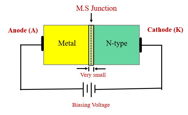
A Schottky diode is formed by the junction of a metal (usually platinum, molybdenum, or chromium) and a semiconductor material (typically n-type silicon). Unlike traditional PN junction diodes, which use a p-n junction, Schottky diodes employ a metal-semiconductor junction. The metal side is called the anode, and the semiconductor side is called the cathode.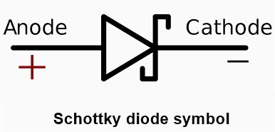
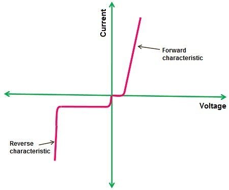
When a forward voltage is applied across the Schottky diode, the metal-semiconductor junction forms a low barrier height, enabling electrons to flow easily from the metal to the semiconductor. This results in a quick and efficient current flow, leading to a fast switching speed and low voltage drop (forward voltage) across the diode.
At lower frequencies, an ordinary diode can easily turn off when the bias changes from forward to reverse. But with the increase in frequency the diode reaches a point where it cannot turn off fast enough to prevent noticeable current during part of the reverse half cycle. The effect is called the charge storage. It restricts the useful frequency of ordinary rectifier diode. How does it happen, it is explained below :
When a diode is forward-biased, some of the carriers in the depletion region have not yet recombined. If the diode is suddenly reverse-biased, the carriers can flow in the reverse for a while. The greater the lifetime, the longer these charges can contribute to reverse current. The reverse recovery time is so short in small signal diodes that its effect cannot be noticed at frequencies below 10 MHz or so. It becomes very important well above 10 MHz. The solution is a special-purpose device called a Schottky diode. Such a diode has no depletion layer eliminating the stored charges at the junction. Because of lack of charge storage the Schottky diode can switch off faster than an ordinary diode. In fact, a Schottky diode can easily rectify frequencies exceeding 300 MHz. Its construction is very different from the normal P-N junction in that a metal-semiconductor junction is developed. On one side of the junction a metal (such as gold, silver, platinum, molybdenum, chrome or tungsten) is used and on the other side of the junction N-type doped silicon (but gallium is often used, especially at high frequencies) is used. Different construction techniques result in different set of characteristics for the device, such as increased frequency range, lower forward bias, and so on.
In both materials, the electrons are the majority carriers. In metal, the level of minority carriers (holes) is insignificant.
Schottky barrier
When the diode is unbiased, electrons on the N-side have low energy levels than electrons in the metal and so the electrons cannot cross the junction barrier, called the Schottky barrier. But when the diode is forward-biased, the electrons on the N-side gain enough energy to cross the junction and enter the metal. Since these electrons plunge into the metal with very large energy, they are usually called the hot carriers and the diode is called the hot-carrier diode.
Construction of a Schottky diode
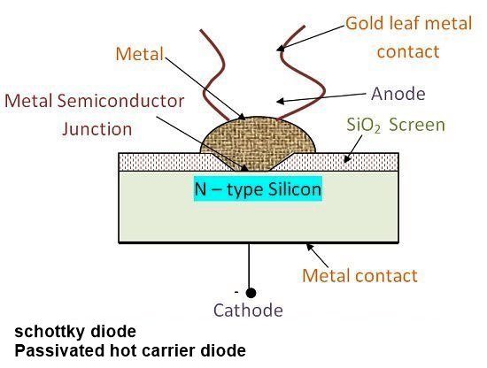
- Semiconductor Material- The semiconductor material used in Schottky diodes is usually n-type silicon. N-type silicon has an excess of free electrons, making it suitable for the formation of the metal-semiconductor junction.
- Metal Contact- A metal contact is placed on the surface of the semiconductor material to form the anode of the Schottky diode. Metals such as platinum, molybdenum, or chromium are commonly used due to their low work functions.
- Metal-Semiconductor Junction- The metal contact is carefully bonded or deposited onto the semiconductor material. This creates the metal-semiconductor junction, also known as the Schottky barrier. The metal side acts as the anode, and the semiconductor side serves as the cathode.
- Barrier Formation- When the metal and semiconductor come into contact, a potential barrier, called the Schottky barrier, is formed at the interface. This barrier arises due to the difference in work functions between the metal and the semiconductor. The metal, having a lower work function, creates a low barrier height at the junction.
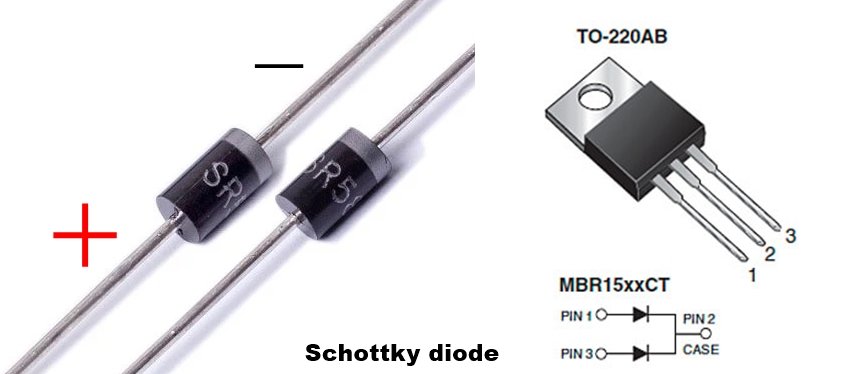
- Package- The Schottky diode is typically housed in a package that provides physical protection and electrical connections. The package may be made of materials such as plastic or ceramic and has external leads for connecting the diode to an electrical circuit.
It’s important to note that the construction of Schottky diodes may vary depending on specific designs and manufacturing processes. Some Schottky diodes may include additional layers or structures to enhance performance or address specific requirements.
Features of Schottky diodes
- Low Forward Voltage Drop– Schottky diodes have a significantly lower forward voltage drop compared to traditional PN junction diodes. The absence of a PN junction and the low barrier height at the metal-semiconductor interface result in minimal voltage loss across the diode. This feature makes Schottky diodes suitable for applications where low power dissipation and high efficiency are desired.
- Fast Switching Speed– Schottky diodes exhibit fast switching characteristics due to their unique structure. The absence of minority carrier storage and recombination effects, which are present in PN junction diodes, enables rapid charge and discharge of the diode. This makes Schottky diodes ideal for high-frequency applications and circuits that require quick switching.
- Low Reverse Recovery Time– Unlike PN junction diodes, Schottky diodes have negligible reverse recovery time (trr). Reverse recovery time refers to the time taken for the diode to switch from the conducting state to the non-conducting state when transitioning from forward bias to reverse bias. The absence of a PN junction depletion region in Schottky diodes eliminates the need for charge removal during the reverse recovery process, resulting in minimal delay and low reverse recovery current.
- High-Temperature Operation– Schottky diodes are capable of operating at higher temperatures compared to PN junction diodes. The absence of a PN junction depletion region and the use of metal-semiconductor junctions allow Schottky diodes to withstand elevated temperatures without significant performance degradation. This feature makes them suitable for applications that require operation in high-temperature environments.
- Small Size and Low Capacitance-Schottky diodes have a smaller physical size compared to PN junction diodes. The absence of a PN junction depletion region allows for a more compact design. Additionally, Schottky diodes exhibit low junction capacitance, enabling their use in high-frequency and high-speed applications. The reduced capacitance helps minimize signal distortion and improves overall circuit performance.
- Wide Range of Voltage Ratings and Current Capacities– Schottky diodes are available in various voltage ratings and current capacities to suit different application requirements. They can be found in a wide range of sizes and packages, making them versatile for use in various electronic circuits and systems.
- Reverse Voltage Limitations– While Schottky diodes offer many advantages, they have a relatively low reverse breakdown voltage compared to PN junction diodes. This restricts their suitability for high-voltage applications. Therefore, careful consideration should be given to the reverse voltage requirements of a specific application when selecting a Schottky diode.
Schottky diode possesses two unique features over an ordinary P-N junction diode viz. (i) It is a unipolar device because of the absence of minority carriers in the reverse direction (no significant current from metal to the semiconductor in reverse-biased condition), while P-N junction diode is a bipolar device as it has both electrons and holes as majority carriers. (ii) Because of the absence of holes in the metal, there is no depletion layer or stored charges to worry about. So Schottky diode can switch off faster than a bipolar diode. Because of the larger contact area between semiconductor and metal its forward resistance is lower (i.e. noise is comparatively lower). The Schottky diode also has a lower barrier potential (about 0.2 -0.25V) whereas normal silicon P-N junction diode has a barrier potential of 0.7 V. This makes it more efficient in high-power applications than silicon rectifiers. However, the Schottky diode do exhibit higher leakage currents and lower reverse breakdown voltages. Consequently, they are only used when reverse recovery time or efficiency are the main concerns.
Applications/uses of Schottky diodes
- Power Supply and Rectification– Schottky diodes are frequently used in power supplies and rectifier circuits. Their low forward voltage drop reduces power losses and improves overall efficiency in converting alternating current (AC) to direct current (DC).
- Switching Applications – Schottky diodes are suitable for high-speed switching applications. Their fast switching speed and low reverse recovery time make them ideal for use in switching regulators, inverters, and other circuits that require quick transitions and minimal power dissipation.
- RF and Microwave Circuits– Due to their low junction capacitance and fast response time, Schottky diodes find application in radio frequency (RF) and microwave circuits. They are used in mixers, detectors, frequency multipliers, and modulators, enabling signal processing and modulation in communication systems.
- Voltage Clamping and Protection– Schottky diodes are employed in voltage clamping circuits and transient voltage suppressors (TVS) to protect sensitive electronic components from voltage spikes and transients. They divert excess voltage and prevent damage to devices during transient events.
- Solar Panels and Photovoltaic Systems– Schottky diodes are commonly used in photovoltaic systems and solar panels. They prevent reverse current flow from the battery or energy storage back to the solar panel, improving overall system efficiency and preventing power loss.
- Automotive Electronics– Schottky diodes find application in automotive electronics, where they are used in alternator rectification, reverse voltage protection, freewheeling diodes, and power supply circuits.
- Data Communication and Networking– Schottky diodes are employed in data communication and networking equipment. They are used in high-speed data transmission circuits, Ethernet switches, routers, and other network infrastructure components.
- Analog and Mixed-Signal Circuits– Schottky diodes are used in analog and mixed-signal circuits for signal conditioning and protection purposes. They find application in signal clamping, peak detection, and analog-to-digital converter (ADC) input protection circuits.
- High-Temperature Environments– Schottky diodes can withstand higher operating temperatures compared to PN junction diodes, making them suitable for use in high-temperature environments. Applications include automotive engine management systems, aerospace electronics, and industrial equipment.
- High-Frequency Rectification– Schottky diodes are well-suited for high-frequency rectification applications. Their low forward voltage drop and fast recovery time make them suitable for use in high-frequency rectifiers, flyback converters, and freewheeling diodes in switching power supplies.
Also read
- PN junction diode
- Zener diode
- What is PIN diode
- What is Optocoupler
- Sample and hold circuit
- Electronics MCQ Quiz

