Contents
What is a photodiode
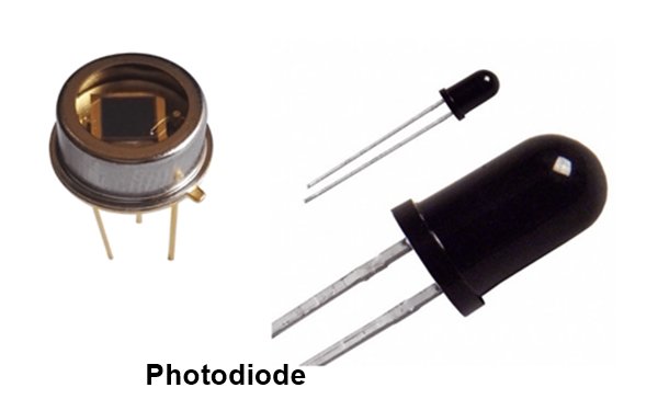
A photodiode is a Two terminal semiconductor device that converts light energy into electrical current. It is a type of photoelectric device widely used in various applications such as light detection, optical communication, and sensing.
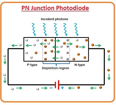
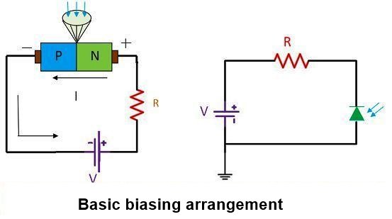
Photodiode is designed to operate in reverse bias. When light photons with sufficient energy strike the photodiode, they can penetrate into the depletion region and generate electron-hole pairs through a process called the photoelectric effect. The electrons are generated in the conduction band of the n-type material, while the holes are generated in the valence band of the p-type material
Construction/Structure of a photodiode
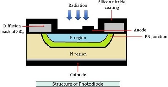
The basic structure of a photodiode consists of a p-n junction, similar to a regular diode. The p-n junction is formed by combining a p-type semiconductor material (with an excess of positively charged carriers, or “holes”) and an n-type semiconductor material (with an excess of negatively charged carriers, or electrons). The junction between these two regions creates a depletion region where no free charge carriers exist.
Photodiodes are constructed using semiconductor materials, primarily silicon (Si) or compound semiconductors like gallium arsenide (GaAs) or indium gallium arsenide (InGaAs). The construction of a photodiode typically involves the following components
Semiconductor Material– Photodiodes are made from a single crystal of semiconductor material, such as silicon. The choice of material depends on the desired properties and applications of the photodiode.
P-N Junction– The semiconductor material is doped to create a p-n junction. Doping involves intentionally introducing impurities into the material to alter its electrical properties. The p-region is doped with acceptor impurities (e.g., boron), which introduce holes, while the n-region is doped with donor impurities (e.g., phosphorus), which introduce free electrons.
Contacts– Metal contacts are placed on the p- and n-regions of the semiconductor material to facilitate electrical connections. These contacts allow for the flow of current generated by the photodiode.
Packaging– Photodiodes are typically enclosed in a package to protect them from external elements and provide mechanical support. The package may have a transparent window to allow incident light to reach the active area of the photodiode.
In addition to these basic components, photodiodes may also incorporate other elements to enhance their performance, such as:
Anti-Reflective Coating– A thin film of anti-reflective material is often applied on the surface of the photodiode to minimize the reflection of incident light. This improves the efficiency of light absorption.
Optical Filters– In some cases, photodiodes may include optical filters to restrict the wavelength range of light that reaches the active area. This helps in selective light detection or suppression of unwanted ambient light.
Optical Windows– Photodiodes used in certain applications, such as high-speed communication, may have specialized optical windows to optimize the interaction between the incident light and the photodiode.
The output voltage is taken from across a series-connected load resistor R. This resistance may be connected between the diode and ground or between the diode and the positive terminal of the supply
Working of photodiode
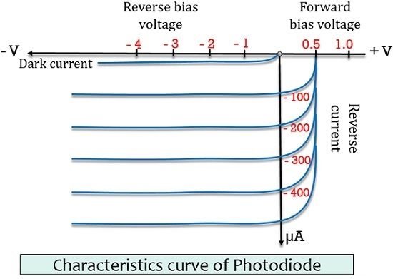
When the P-N junction is reverse-biased, a reverse saturation current flows due to thermally generated holes and electrons being swept across the junction as the minority carriers. With the increase in temperature of the junction more and more hole-electron pairs are created and so the reverse saturation current I0. increases. The same effect can be had by illuminating the junction. When light energy bombards a PN junction, it dislodges valence electrons. The more light striking the junction the larger the reverse current in a diode. It is due to the generation of more and more charge carriers with the increase in level of illumination. The dark current is the current that exists when no light is incident. It is to be noted here that current becomes zero only with a positive applied bias equals to V0. The almost equal spacing between the curves for the same increment in luminous flux reveals that the reverse saturation current I0 increases linearly with the luminous flux. An increase in reverse voltage does not increase the reverse current significantly, because all available charge carriers are already being swept across the junction. For reducing the reverse saturation current I0 to zero, it is necessary to forward bias the junction by an amount equal to barrier potential. Thus the photodiode can be used as a photoconductive device.
On. Removal of reverse bias applied across the photodiode, minority charge carriers continue to be swept across the junction while the diode is illuminated. This has the effect of increasing the concentration of holes in the P-side and that of electrons in the N-side. But the barrier potential is negative on the P-side and positive on the N-side and was created by holes flowing from P to the N-side and electrons from N to the P-side during fabrication of the junction. Thus, the flow of Minority carriers tends to reduce the barrier potential.
When an external circuit is connected across the diode terminals, the minority carriers return to the original side via the external circuit. The electrons, which crossed the junction from P to N-side, now flow out through the N-terminal and into the P-terminal. This means that the device is behaving as a voltage cell with the N-side being the negative terminal and the P-side the positive terminal. Thus, the photodiode is a photovoltaic device as well as the photoconductive device. When the device is operated with a reverse bias, it operates as a photoconductive device and when operated without the reverse bias, it operates as a photovoltaic device. Since the rise and fall times (change-of-state parameters) are very small for this device (in the nanosecond range), it can be employed for high-speed counting or switching applications.
Photodiodes have a far lower light sensitivity than cadmium sulphide LDRs, but give a fair quicker response in light level. Generally, LDRs, are ideal for use in slow-acting direct coupled light-level sensing applications, while photodiodes are ideal for use in fast-acting ac coupled signaling applications.
Applications of Photodiode
Typical photodiode applications include detection (both visible and invisible),
Light Detection– Photodiodes are widely used for detecting and measuring light intensity in applications such as ambient light sensors, light meters, exposure control in cameras, and optical power meters.
Optical Communication– Photodiodes play a crucial role in optical communication systems, where they are used as receivers to convert optical signals carrying data into electrical signals. They are used in fiber optic communication networks, high-speed data transmission, and telecommunications.
Remote Control Systems– Many remote control systems, such as those used for TVs, DVD players, and other electronic devices, utilize infrared (IR) photodiodes to receive signals from the remote control unit.
Barcode Scanning– Photodiodes are employed in barcode scanners, where they detect the reflected light from barcodes and convert it into electrical signals for decoding.
Proximity and Motion Sensing– In proximity sensors and motion detection systems, photodiodes are used to detect changes in light intensity caused by the presence or movement of objects. They are found in automatic doors, occupancy sensors, and security systems.
Medical Instruments– Photodiodes are used in medical instruments and devices for applications such as pulse oximetry, where they measure the oxygen saturation level in a patient’s blood.
Automotive Applications– Photodiodes are employed in automotive applications for tasks such as ambient light sensing, automatic headlight control, rain sensors, and collision detection systems.
Environmental Monitoring– Photodiodes are used in environmental monitoring systems to measure and analyze various parameters such as UV radiation, solar radiation, and air quality.
Industrial Applications– Photodiodes are used in industrial applications for tasks such as quality control, position sensing, level detection, and object detection.
Scientific Research– Photodiodes are utilized in scientific research for light detection and measurement in various experiments and instruments.
Avalanche photodiode (APD)
An avalanche photodiode (APD) is a type of photodiode that utilizes a process called avalanche multiplication to achieve higher sensitivity and lower noise compared to a regular photodiode.
Working principle
In an APD, incident photons generate electron-hole pairs within the semiconductor material, similar to a regular photodiode. However, the unique feature of an APD lies in its ability to achieve avalanche multiplication.
Avalanche multiplication occurs in a region of the APD called the multiplication region. This region is heavily doped and designed to create a high electric field. When a photon-generated carrier enters the multiplication region, it gains enough energy from the electric field to cause impact ionization.
During impact ionization, the high-energy carrier collides with the atoms of the semiconductor material, creating additional electron-hole pairs. These newly generated carriers can then undergo further impact ionization, resulting in an exponential increase in the number of electron-hole pairs.
This avalanche multiplication effect significantly amplifies the original photocurrent, leading to higher sensitivity to low-light levels. The gain achieved through avalanche multiplication depends on the bias voltage applied to the APD. However, it is important to note that operating an APD at high voltages can increase noise levels and may require careful optimization for optimal performance.
Avalanche photodiodes are commonly used in applications where high sensitivity and low noise are crucial, such as low-light imaging, long-distance optical communication systems, and high-speed data transmission. They are also utilized in scientific research, industrial applications, and other fields that require the detection of weak optical signals.
Structure and construction of Avalanche photodiode
This diode includes two heavily doped & two lightly doped regions. Here, heavily doped regions are P+ & N+ whereas lightly doped regions are I & P.
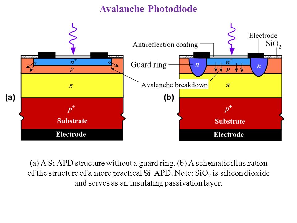 Avalanche Photodiode Construction
In the intrinsic region, the depletion layer width is fairly thinner in this diode as compared to the PIN photodiode. Here, the p+ region works like the anode whereas the n+ region acts as the cathode.
As compared to other photodiodes, this diode works in a high reverse bias condition. So this allows avalanche multiplication of the charge carriers formed through the light impact or photon. The avalanche action allows the gain of the photodiode to be enhanced several times to provide a high range of sensitivity.
Advantages of avalanche photodiode
Avalanche photodiodes (APDs) offer several features and advantages that make them suitable for specific applications. Here are some of the key features and advantages of APDs:
- Higher Sensitivity– APDs provide higher sensitivity compared to regular photodiodes. The avalanche multiplication effect allows for the amplification of the photocurrent, enabling APDs to detect and measure very low levels of light.
- Low Noise– APDs exhibit lower noise characteristics, particularly in the presence of low light levels. The avalanche multiplication process helps to reduce the impact of noise sources, resulting in improved signal-to-noise ratio.
- Wide Dynamic Range– APDs can operate over a wide range of light intensities. They can detect both weak signals in low-light conditions and strong signals without saturating, making them suitable for applications that require a broad dynamic range.
- Fast Response Time– APDs typically have fast response times, allowing for quick detection and measurement of light signals. This makes them suitable for high-speed applications such as optical communications and time-resolved measurements.
- High Quantum Efficiency– APDs can achieve high quantum efficiency, meaning they are capable of converting a high percentage of incident photons into electrical current. This is advantageous for applications that require high detection efficiency.
- Compact Size– APDs can be designed in compact sizes, allowing for integration into small form-factor devices and systems. This makes them suitable for applications where space is limited, such as portable devices and optical modules.
- Temperature Stability– APDs can exhibit good temperature stability, maintaining their performance characteristics over a wide range of operating temperatures. This stability is beneficial in environments with varying temperature conditions.
- Wavelength Range– APDs can be designed to operate across a wide range of wavelengths, from visible light to near-infrared (NIR) and even longer wavelengths. This flexibility allows for their use in various applications across different spectral regions.
Disadvantages of Avalanche Photodiodes (APDs):
- Higher Bias Voltage Requirements– APDs require a higher bias voltage compared to regular photodiodes to initiate and sustain the avalanche multiplication effect. This increased bias voltage can impact the power consumption and complexity of the driving circuitry.
- Temperature Sensitivity– APDs can be sensitive to temperature variations, which can affect their performance. Temperature control and stabilization may be necessary to maintain optimal operation.
- Excess Noise– While APDs exhibit lower noise characteristics overall, they can be susceptible to excess noise phenomena, such as after pulsing and thermal noise. Careful design and optimization are required to minimize these noise sources.
- Cost– APDs tend to be more expensive compared to regular photodiodes. The specialized design, manufacturing processes and higher quality requirements contribute to their higher cost.
Also read
-
What is opt coupler/opto-isolator
-
Infrared proximity sensor circuit
-
Half wave and Full wave rectifier
-
Darkness detector circuit using LDR and Photodiode
-
IR Remote controlled ON-OFF switch circuit

