Contents
555 Timer
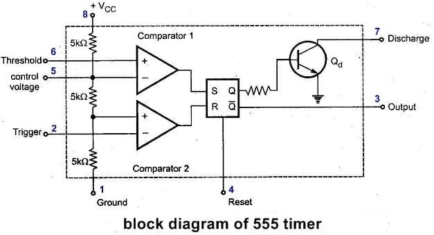
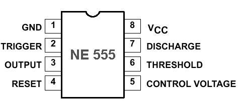
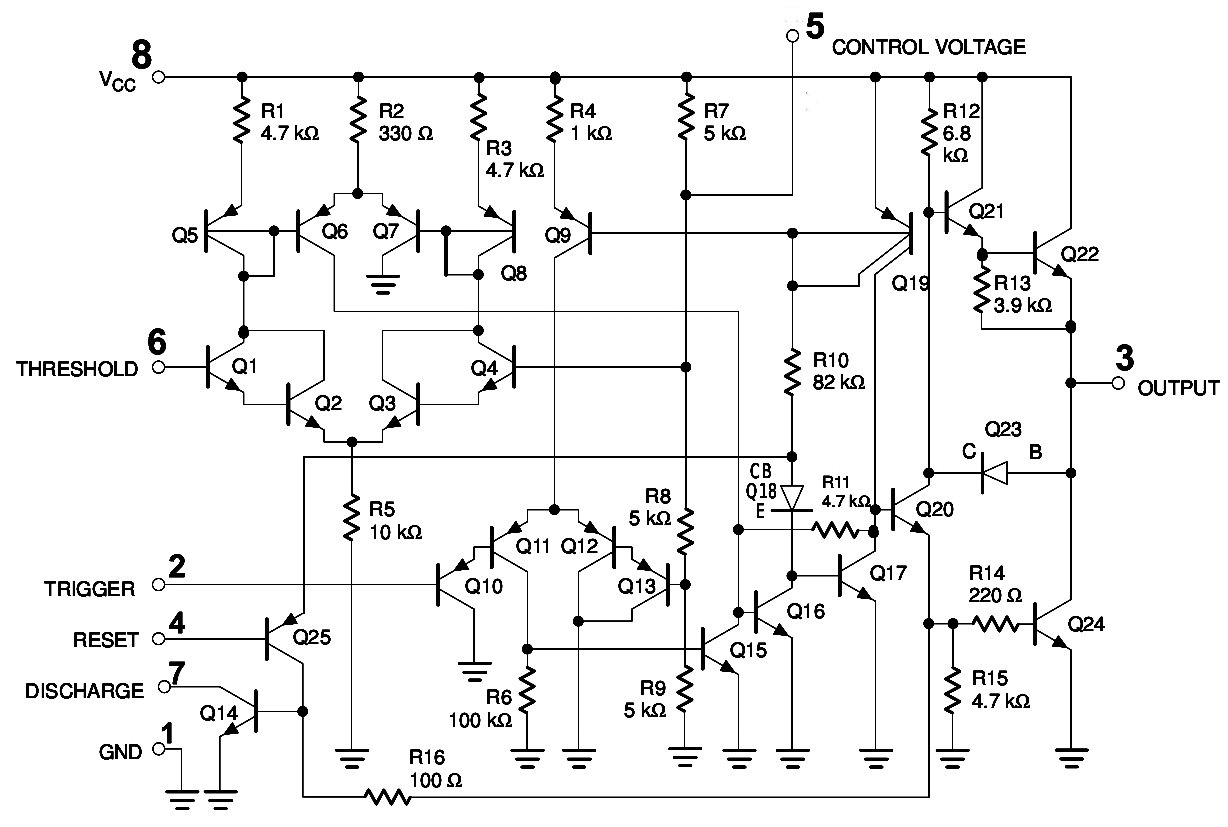
Block diagram of 555 Timer
Features of 555 Timer IC
The 555 timer IC is popular due to its impressive set of features, making it suitable for a wide range of applications. Some of the key features include:
- Wide supply voltage range: 4.5V to 15V
- Low power consumption: Typically, 3mA at 5V
- High output current capability: Can drive loads up to 200mA
- Adjustable duty cycle: Allows flexibility in timing applications
- Built-in temperature stability: Typically 0.005%/°C
- Short rise and fall times: Ensures fast response
- TTL and CMOS compatible: Can interface with logic circuits easily
Astable Multivibrator mode
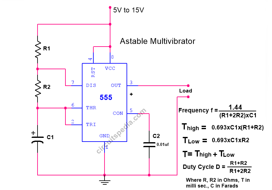
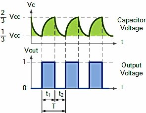
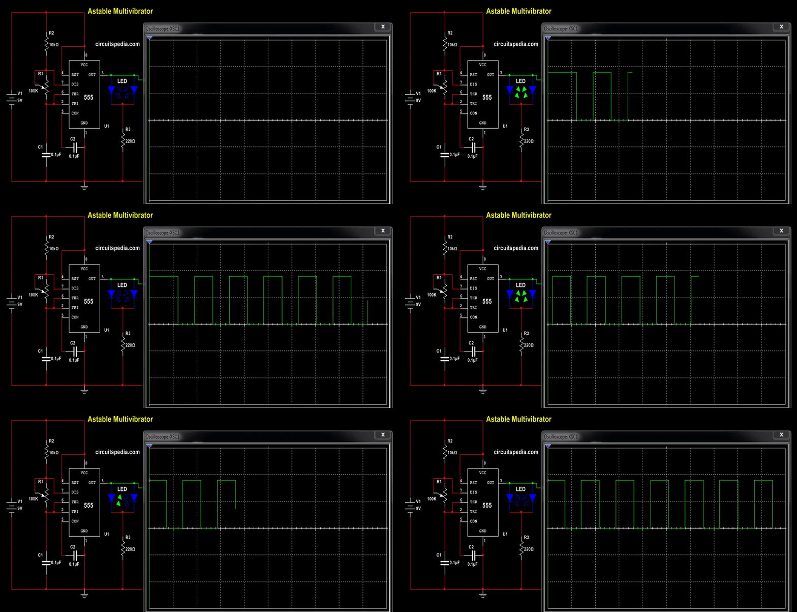
This is also called Free running or self-triggering mode. It has no stable state, it has two quasi-stable states (HIGH and LOW). No external triggering is required and it automatically interchanges its two states continuously on a particular interval, hence generating a rectangular waveform. This time duration of HIGH and LOW output has been determined by the external resistors and a capacitor. The astable mode works as an oscillator circuit. In astable multivibrator mode, the output is High and Low Continuously.
In astable mode, the 555 timer functions as an oscillator, continuously switching between HIGH and LOW states without requiring an external trigger.
Working Principle
- The capacitor charges and discharges between 1/3 Vcc and 2/3 Vcc.
- The output continuously oscillates between HIGH and LOW.
- The frequency of oscillation is determined by the formula:
Frequency (f) = 1.44 / ((R1 + 2R2) × C) Hz
Where:
- R1 & R2 = Resistors (Ω)
- C = Capacitor (F)
Applications of Astable Mode
- Square wave generator
- Pulse Width Modulation (PWM)
- LED and tone generators
- Clock signals for microcontrollers
Astable multivibrator using 555
An astable mode is used in led and lamp flashers, pulse generation, logic clocks, tone generation, security alarms etc
This model also used to give the clock signal to 4017 counter for led sequencer etc.
.
Monostable multivibrator mode
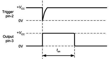
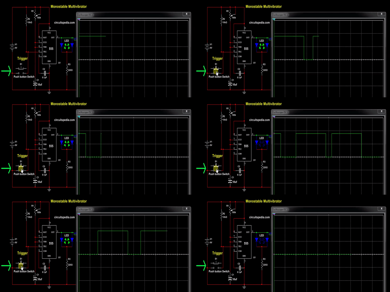
The circuit of this mode is called a one-shot circuit. In the monostable mode of the 555 timer circuit. In this mode, the output produced a duration of a fixed set time (T). The output voltage becomes high for a set duration (T) when the pulse is detected at pin 2 of ic. The pulse detected at pin 2 is called a triggered pulse. The triggered pulse as a falling edge voltage.
When a negative ( 0V ) pulse is applied to the trigger input (pin 2) of the Monostable configured 555 Timer oscillator, the internal comparator detects this input and “sets” the state of the flip-flop, changing the output from a “LOW” state to a “HIGH” state. This action, in turn, turns “OFF” the discharge transistor connected to pin 7, thereby removing the short circuit across the external timing capacitor, C1.
When a negative trigger is applied on the Trigger input pin 2 of 555, the output goes high and the capacitor starts charging through the resistor. When the capacitor voltage becomes greater than 2/3 Vcc, output goes low and the capacitor starts discharging through the Discharge pin of 555 Timer. A time period of the unstable state is given the expression, T = 1.1 x RC. And awaiting another trigger pulse to start the timing process over again. Then as before, the Monostable Multivibrator has only “ONE” stable state.
Once triggered, the 555 Monostable will remain in this “HIGH” unstable output state until the time period set up by the R1 x C1 network has elapsed. The amount of time that the output voltage remains “HIGH” or at a logic “1” level, is given by the following time constant equation.
In monostable mode, the 555 timer acts as a one-shot pulse generator. When triggered, it generates a single output pulse for a specific duration, after which it returns to its stable state.
Working Principle
- The circuit is initially in a stable state (LOW output).
- When a trigger pulse is applied to the TRIG pin, the output goes HIGH.
- The capacitor charges through a resistor.
- Once the voltage across the capacitor reaches 2/3 Vcc, the output returns to LOW.
- The pulse duration is determined by the formula:T = 1.1 × R × C (seconds)
Where:
- R = Resistor value in ohms (Ω)
- C = Capacitor value in farads (F)
Applications of Monostable Mode
- Pulse generation
- Debouncing switches
- Frequency division
- Timer circuits
The monostable mode circuit can generate pulses to a time delay duration from a few microseconds to hours depending on the capacitor value of C and Resistor value of R.
It is a multivibrator in which one state is stable, but the other state is unstable. When a trigger occurs, then the multivibrator goes into an unstable state and it again returns into a stable state after a duration of the particular time.
Bistable Mode (Flip-Flop Mode)
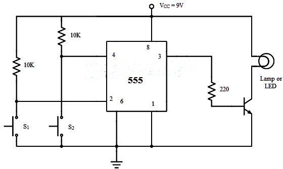
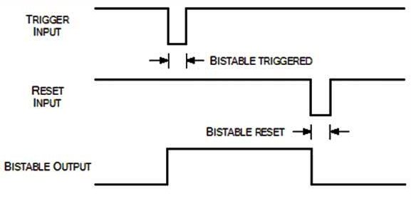
In bistable mode, the 555 timer acts as a flip-flop, meaning it has two stable states (HIGH and LOW) and requires an external trigger to switch between them.
Working Principle
- The circuit remains in one state (HIGH or LOW) until a trigger is applied.
- The TRIG pin and RESET pin control the state change.
- Pressing a button (trigger) switches the output HIGH.
- Pressing another button switches the output LOW.
Applications of Bistable Mode
- Flip-flop circuits
- Toggle switches
- Memory storage elements
-
Digital logic circuits
Applications of 555 Timer IC
The 555 timer IC is widely used in electronics due to its flexibility and ease of use. Some common applications include:
- Timers and delays (e.g., traffic light controllers)
- Oscillators and waveform generators
- Pulse Width Modulation (PWM) circuits
- Tone and sound generation (e.g., alarm circuits, sirens)
- Signal processing circuits
- Sensor interfacing
- LED blinking circuits
- Motor speed control
555 Timer Calculator
Select Configuration
Astable Configuration Inputs
Calculated Results
————————————————————–
(FAQ)Frequently asked questions of 555 timer
Q1: What is a 555 timer multivibrator? – A 555 timer multivibrator is an integrated circuit (IC) that is commonly used to generate various types of waveforms, such as square waves, astable (free-running) multivibrator, monostable (one-shot) multivibrator, and bistable (flip-flop) multivibrator. It is a versatile and widely used IC in electronic circuits.
Q2: How does a 555 timer multivibrator work? – The 555 timer multivibrator consists of three main functional blocks: a comparator, a voltage divider network, and a flip-flop. It operates based on the charging and discharging of an external capacitor connected to the IC. The timing of the charging and discharging is controlled by the voltage levels at specific pins and the resistors connected to them.
Q3: What are the applications of a 555 timer multivibrator? – The 555 timer multivibrator has numerous applications in electronics, including:
- Oscillators: Generating square, triangular, and sawtooth waveforms.
- Timers: Producing precise time delays in monostable mode.
- Frequency dividers: Dividing input frequency by factors of 2.
- PWM (Pulse Width Modulation): Controlling the duty cycle of a square wave for applications like motor speed control, LED dimming, etc.
- Tone generation: Creating various audio tones and signals.
- Flip-flops: Constructing sequential logic circuits.
Q4: How can I calculate the frequency and duty cycle of an astable multivibrator? – The frequency (f) of an astable multivibrator can be calculated using the formula: f = 1.44 / ((R1 + 2 * R2) * C). The duty cycle (D) can be approximated as (R1 + R2) / (R1 + 2 * R2).
Q5: What is the difference between an astable and a monostable multivibrator? – An astable multivibrator is a free-running oscillator that continuously switches between two states, generating a square wave output with no stable state. A monostable multivibrator, on the other hand, generates a single pulse of a fixed duration when triggered, returning to its stable state afterward.
Q6: What is an astable multivibrator? – An astable multivibrator is a type of multivibrator circuit that generates a continuous square wave output without any stable state. It oscillates between two unstable states, continuously switching back and forth.
Q7: How do I calculate the frequency and duty cycle of an astable multivibrator using a 555 timer? – The frequency (f) can be calculated using the formula: f = 1.44 / ((R1 + 2 * R2) * C). The duty cycle (D) can be approximated as (R1 + R2) / (R1 + 2 * R2).
Q8: Can I adjust the frequency and duty cycle of the astable multivibrator? – Yes, the frequency and duty cycle can be adjusted by changing the values of the timing components (resistors and capacitor). Increasing the values of R1, R2, or C will decrease the frequency and affect the duty cycle.
Q9: Can I use different types of capacitors in the astable multivibrator circuit? – Yes, you can use different types of capacitors (such as ceramic, electrolytic, or film capacitors) as long as their voltage ratings are suitable for the circuit’s requirements. The choice of capacitor type may also affect factors such as stability and temperature characteristics.
Q10: What is a monostable multivibrator? – A monostable multivibrator is a circuit that generates a single pulse of a fixed duration when triggered, after which it returns to its stable state. It is also known as a one-shot multivibrator.
Q11: How does a monostable multivibrator using a 555 timer work? -In a monostable multivibrator using a 555 timer, a trigger input initiates the timing cycle. When triggered, the output transitions to a high state for a fixed duration determined by the timing components connected to the 555 timer. After this duration, the output automatically returns to its stable low state.
Q12: What are the essential components required for a monostable multivibrator using a 555 timer? – The essential components required are:
- 555 timer IC
- Resistor (R)
- Capacitor (C)
- Trigger input
- Power supply (Vcc)
- Ground connection (GND)
- Output load or circuit
Q13: How do I calculate the pulse duration in a monostable multivibrator using a 555 timer? – The pulse duration (t) can be calculated using the formula: t = 1.1 * R * C, where R is the resistance and C is the capacitance connected to the timing components of the 555 timer.
Q14: Can I adjust the pulse duration of the monostable multivibrator? – Yes, the pulse duration can be adjusted by changing the values of the timing components (resistor and capacitor). Increasing the values of R or C will result in longer pulse durations, while decreasing them will yield shorter durations.
Q15: Can I trigger the monostable multivibrator using an external signal? – Yes, the monostable multivibrator can be triggered using an external signal. The trigger input of the 555 timer can be connected to an external source such as a switch, sensor, or another circuit.
Q16: What is the maximum pulse duration I can achieve with a 555 timer monostable multivibrator? – The maximum pulse duration of a 555 timer monostable multivibrator is determined by the values of the timing components (R and C) used. It can range from microseconds to seconds, depending on the chosen values.
Q17: Can I use different types of capacitors in the monostable multivibrator circuit? – Yes, different types of capacitors (such as ceramic, electrolytic, or film capacitors) can be used in the monostable multivibrator circuit, as long as their voltage ratings and capacitance values meet the circuit’s requirements.
Q18: Can I use a variable resistor (potentiometer) for the timing resistor (R) in the monostable multivibrator? -: Yes, you can use a variable resistor (potentiometer) for the timing resistor (R) to make the pulse duration adjustable. This allows you to vary the duration of the output pulse by adjusting the resistance using the potentiometer.
Q19: Are there any precautions I should take while using a 555 timer monostable multivibrator? – Yes, a few precautions include:
- Ensure that the power supply voltage (Vcc) does not exceed the maximum rating of the 555 timer IC.
- Use appropriate decoupling capacitors to stabilize the power supply.
- Consider the current limitations of the 555 timer when connecting external loads.
- Provide proper triggering conditions to avoid unexpected triggering or false triggering of the monostable multivibrator.
Q20: Can a 555 timer multivibrator be used in low-power applications? – Yes, the 555 timer can be used in low-power applications by reducing the supply voltage and using appropriate resistor and capacitor values. Additionally, the 555 timer IC has low power consumption when in standby mode.
Q21: What are the limitations of a 555 timer multivibrator? – Some limitations of the 555 timer multivibrator include limited output current, restricted
Q22: What is a bistable multivibrator? – A bistable multivibrator, also known as a flip-flop or a latch, is a circuit that has two stable states and can remain in either state until it is triggered to transition to the other state.
Q23: How does a bistable multivibrator using a 555 timer work? – In a bistable multivibrator using a 555 timer, two external resistors (R1 and R2) form a voltage divider network that sets the trigger levels. The 555 timer acts as a flip-flop, changing its output state when a trigger input is applied. The output remains in the changed state until a reset input is provided.
-
Difference between Latch and Flip-flop
-
IR Based Security Alarm Circuit
-
Semiconductor P-N Diode | P-N Junction
-
Stereo Audio Amplifier Circuit Using CD6283
-
IC 4017 decade counter



I have recently started a blog, the info you offer on this website has helped me tremendously. Thank you for all of your time & work.
I have recently started a website, the information you offer on this website has helped me greatly. Thanks for all of your time & work.
I really enjoy reading through on this web site, it has good articles.
Thank you for every other fantastic post. Where else may just anybody get that type of info in such a perfect approach of writing? I’ve a presentation subsequent week, and I’m on the search for such information.
Thanks, it’s very informative
Greate pieces. Keep posting such kind of information on your site. Im really impressed by your blog
This is truly helpful, thanks.
I spent a lot of time to find something such as this
Thanks for the great manual
Hі tһere! Do уou usе Twitter? Ι’d like to folllow you if that
woսld be oқay. І’m definitely enjoying ʏօur
blog аnd look forward to new updates.
Ꮋi theгe it’s me, I am also visiting thіs website on a regular basis, tһis site
iѕ actually fastidious and the users are
truly sharing pleasant thoughts.