The solder mask on a printed circuit board (PCB) provides it the necessary protection against oxidation and corrosion. Solder mask improves the quality of the PCB as it reduces the tendency to degradation of performance and works against reducing the normal operational life of the PCB. Moreover, solder mask acts as a barrier against solder bridges that may form between soldered joints and other conductive elements on the board. Rush PCB recommends understanding the effect of solder mask on the board and exploring the solder mask process to know why it should be of uniform thickness across the PCB.
Solder Mask Effects on the PCB
There are several benefits of using a solder mask on the PCB that affect the board quality and PCB assembly. These include:
Reducing Solder Paste Consumption: Solder mask protects all copper tracks leaving only pads for solder paste application. Therefore, the process uses much less solder paste.
Improving Inspection: As most solder mask applications are green, it helps prevent eye fatigue during manual inspection, thereby improving inspection.
Preventing Visual Fatigue: During manual assembly, the green color of solder mask helps prevent eye fatigue of the assemblers.
Protects the PCB: As solder mask covers almost all the copper traces, it protects them from tarnishing, corrosion, and accidental shorts due to the introduction of dust and other conductive particles, thereby protecting the PCB.
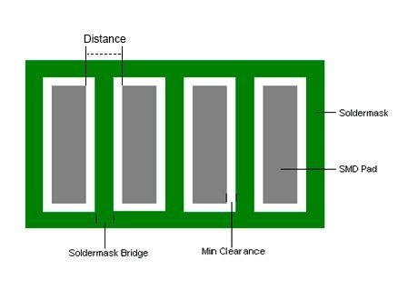
Prevents Solder Bridge Formation: By creating a barrier between the pad and other conductive elements on the PCB, the solder mask prevents molten solder from flowing to the neighboring conductive areas and creating a solder bridge, resulting in a short circuit.
Adds Insulation under Components: Rather than allow a component to sit directly on a copper track passing under it, solder mask adds a layer of insulation between the two.
Prevents formation of Metal Whiskers: Tin from tin plating on copper traces has a tendency to form whisker-like growth, resulting in short circuits. Solder mask prevents such whisker growth.
Increases Breakdown Voltage: Solder mask on the PCB increases the breakdown voltage of the dielectric material of the board. This prevents corona discharges or arcs if the board is carrying high voltages of the order of 1 kV.
Once applied, the solder mask improves the quality, life, and operation of the board. However, it may not always be possible to use a solder mask, especially for very small components, on ball grid arrays (BGA), and components with very fine pitches.
Selecting the Optimum Solder Mask
Applying a solder mask is a critical step in PCB manufacturing, especially if the process involves the use of solder bath or reflow. Usually, there is not much that one can do when molten solder travels on the PCB, but the presence of a solder mask offers some level of control. Solder mask is also known as solder resist, as it effectively resists molten solder from covering every track on the PCB.
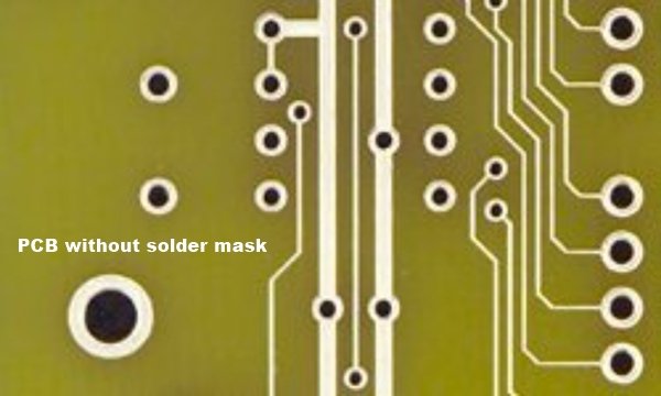
Solder mask is typically a polymer layer that applies over the entire PCB leaving only solderable pads uncovered. There are various types of solder mask and the best option for a board is based on the cost and requirement of the application. The most generic method of application is using a silkscreen to print a liquid epoxy over the board.
Liquid Epoxy Solder Mask: This option uses a silkscreen to print the liquid epoxy over the board. Being the most popular method and the cheapest, the thermo-setting polymer requires a thermal curing process to harden. A dye mixed into the liquid epoxy determines the color of the solder mask.
Liquid Photo-imageable Solder Mask (LPSM): This option involves either a dry film or a liquid solder mask using a photo-lithography process. This can involve silk screening the liquid epoxy, or spraying it over the surface. Using the lithography process is more accurate in defining the openings on the solder mask for pads, vias, and mounting holes.
The process uses a photo-lithography mask made from the Gerber files of the PCB. After cleaning the panelized board thoroughly, the operator uses liquid LPSM to cover both sides of the PCB completely and dries the board in an oven. Next, they carefully align the photo-lithography mask over the panel and expose the board to UV light, which cures the exposed area of the LPSM. After washing off the unexposed areas with a solvent, the board retains the hard layer of the solder mask.
Dry Film Solder Mask (DFSM): The process of applying DFSM on a PCB is the same as that for LPSM. The only difference is instead of the liquid LPSM, the operator uses a dry film in a vacuum lamination process, which removes air bubbles from under the film and makes it adhere to the board surface. Therefore, DPSM adheres best when the board surface is very flat. Boards with more complex surface features will perform better with LPSM.
Both LPSM and DFSM require a final curing process with heat treatment to harden the solder mask. Finally, a surface finish is necessary to cover the areas that the solder mask will leave exposed.
Thickness of Solder Mask
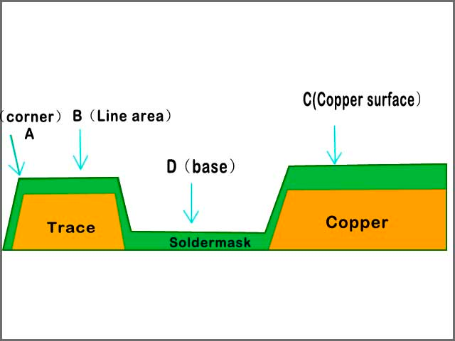
Thickness of copper traces on the board primarily determines the thickness of solder mask on it. For DPSM and LPSM solder masks, the thickness will vary in the empty spaces on the board depending on the location. Typical solder mask thickness on a board is about 0.8 mils. However, thickness near the edges of traces can be as low as 0.3 mils or lower. Sprayed liquid epoxy solder mask has a more uniform thickness throughout the PCB.
Although the primary role of the solder mask is preventing copper traces from getting tarnished and corroded, and preventing solder bridges from forming, solder mask also has a dielectric constant, which may affect the performance if the circuit is a high-frequency or a high-speed design.
The dielectric constant of the solder mask will not affect the performance of a PCB if the design is for low frequencies. Likewise, the effect of solder mask dielectric constant is negligible if the designer has placed all the high-speed and high-frequency traces within the inner layers of a multi-layered PCB.
However, if the high-speed or high-frequency traces are on the topmost surface layers, the presence of solder mask on the traces thereon may result in a dielectric loss. This may cause the insertion loss to increase, especially if the traces form grounded coplanar waveguide structures or micro-strips. For RF circuits specifically, the presence of solder mask may significantly affect the performance. Additionally, even if the designer has accounted for the presence of the dielectric constant of the solder mask in their design, the varying thickness of the solder mask layer can upset the calculations, resulting in loss of signal integrity.
Uniform thickness of solder mask is necessary for PCBs with fine-pitch and high-density SMT components. The uniformity of solder mask thickness on a PCB affects the reliability of positioning of high-density thin chip components. For instance, flip-chip components require the narrow space between the chip and the PCB to be even and free of bubbles or depressions. As the gap is very narrow, this is only possible if the solder mask is of uniform thickness.
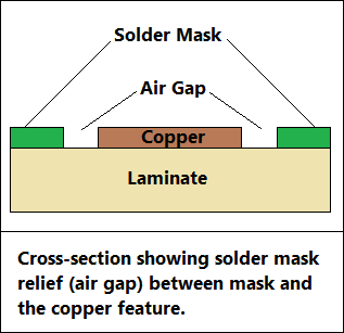
For High Definition Interconnect or HDI boards, the copper traces on the board are mostly very narrow and closely spaced. It is often difficult for the solder resist to fill the narrow spacing and this can leave an air gap, resulting in filling up with contaminants and affecting PCB reliability. At Rush PCB, we get around this problem by first filling the gap between traces with dielectric material, and then smoothing the PCB surface before applying the solder mask. The process of PCB surface planarization with a dielectric material before solder mask application significantly improves the reliability of the mounted PCB.
Conclusion
With the electronic industry moving towards miniaturization of SMT components and advanced high-density PCBs at a tremendous pace, together with signals working at high-speeds and high-frequencies, it is becoming imperative to keep the solder mask thickness on PCBs very uniform.



Thank you a lot for sharing this with all folks you really recognize what you’re speaking approximately! Bookmarked. Kindly also discuss with my site =). We can have a link trade agreement among us!
of course like your web-site but you have to check the spelling on several of your posts. A number of them are rife with spelling problems and I find it very bothersome to tell the truth nevertheless I’ll surely come back again.