Sample and hold circuit
Definition and Introduction
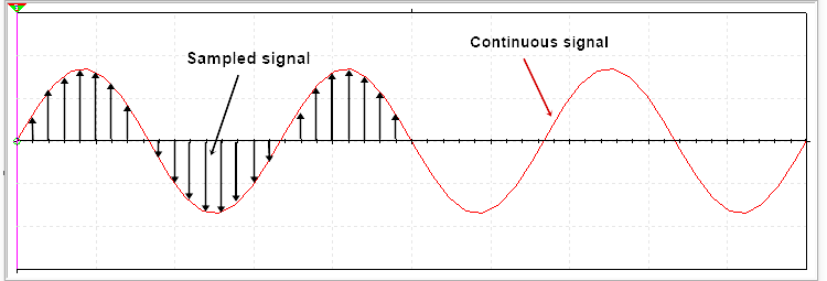
A sample and hold circuit is an electronic circuit that makes samples of input voltage signals and holds these samples signal for a very small time duration.
A sample and hold circuit is basically an analog-to-digital converter circuit. Input voltage signals are sampled and held for some duration (in microseconds) using the capacitor, and the output is in the form of a digital pulse. Because this works by holding the sampled analog input signal, this is called the sample and hold circuit. Holding of the signal is done using a capacitor called a holding capacitor. The capacitor has the ability to store the voltage by charging until it discharges. This charging and storing property of the capacitor is used here for holding the signal.
Sample
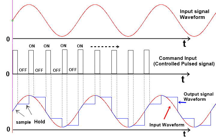
Some Parts consider or take the values of a given continuous input signal at each different time is called a sample.
Hold
catch the sampled signals and take hold for a time t is called hold.
Sampling time
The time during which the samples of input signals are generated is called sampling time. This is usually 1 us to 14 u sec.
Holding time
The time during which the circuit holds the sampled value is called the holding time. Holding time to be set according to the required for application.
Basic sample and holding circuit
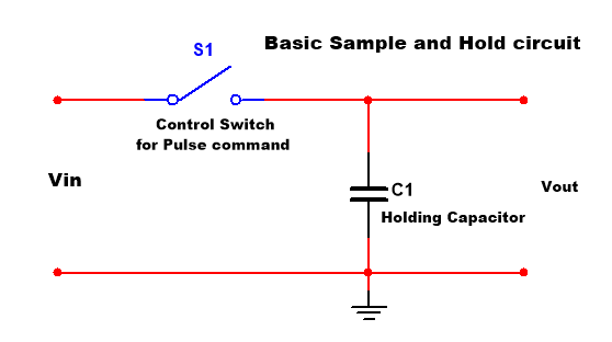
A basic sample and hold circuit consists of a switch and a capacitor. A combination of a control switch and a capacitor is called a simple sample-and-hold circuit. Input voltage is applied at the point Vin, and then a switch is connected. After that, a capacitor is connected between the switch and the output. One side of the capacitor is connected to the ground. A JFET or a MOSFET is used as a Control switch.
Working
When the switch is closed, the connected capacitor is charged, and when the switch is opened, the capacitor will not get discharged because there is no path for discharging, and then the capacitor takes to hold the signal.
Sample and hold circuit using op-amp
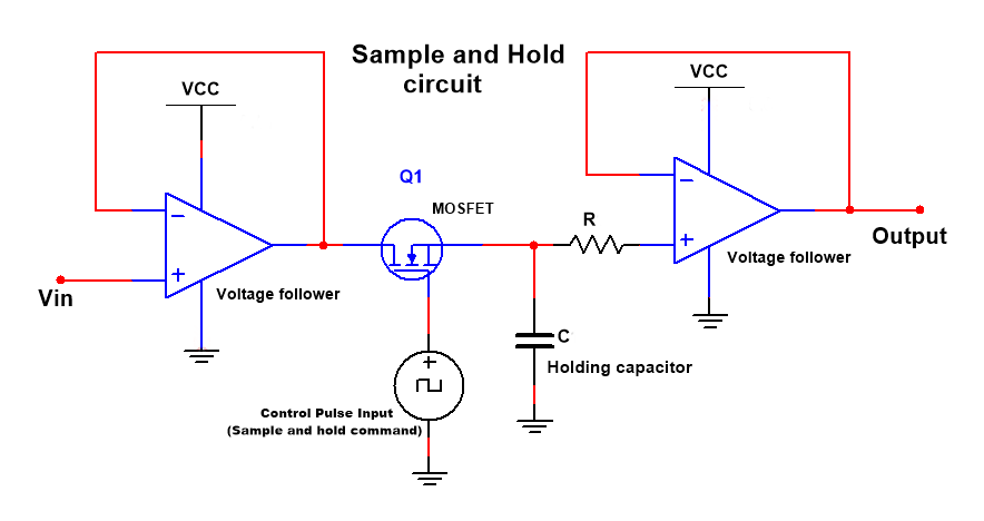
In this circuit, two voltage follower circuits, a capacitor, and A MOSFET are connected. The input voltage given at the control voltage is given on the gate terminal of the MOSFET; here, the MOSFET is used as a switch. The reason of using the Voltage follower circuit is that this circuit gives an output the same as the input signal, and there is a very high input impedance, so no load is considered at the input, and the capacitor will also not get discharged because of the very high impedance at the input of the op-amp.
The MOSFET is used here as the control switch for applying the voltage pulse. The Gate terminal of the MOSFET is connected with a controlled pulsed signal generator. A stable multivibrator can be used to produce a frequency. This astable frequency switch ON-OFF Very fast, the MOSFET. By the ON-OFF, ON-OFF of the MOSFET, a pulsed form of the input voltage signal is applied to the NON-inverting terminal of the Op-amp. The capacitor will charge as a pulse signal gets the 1st pulse to its max level, and this level is held for a definite time by the capacitor because this capacitor will not discharge. Now the next pulse falls, and the capacitor will again charge as this pulse voltage level. and this level holds, and this process is continuously proceeding as per pulse signal and the amplitude level of the pulse signal.
So, in this whole process, the output is sampled and also held for a time duration; these are done by the main capacitor used in this circuit. We know that the sampled signals are the digital signals, so we can say that the sample and hold circuit converts analog or continuous-time signals into digital signals.
Uses or applications of Sample and Hold circuit
- ADCs (Analog-to-Digital Conversion)
- DACs (Digital-to-Analog Conversion)
- In Analog Demultiplexing
- In Linear Systems
- In Data Distribution System
- In Digital Voltmeters
- In Signal Constructional Filters
Simulation Video On Multisim
FAQ on Sample and Hold Circuit
1. What is a Sample and Hold (S&H) Circuit?
A Sample and Hold (S&H) circuit captures (samples) an analog signal at a specific time and holds (maintains) that value for a certain period, usually for conversion by an ADC (Analog-to-Digital Converter).
2. What is the main purpose of a Sample and Hold Circuit?
The primary purpose is to capture and stabilize fast-changing analog signals so that an ADC or other processing unit can accurately process them.
3. How does a Sample and Hold Circuit work?
- The circuit consists of a switch (MOSFET or JFET), a capacitor, and an operational amplifier (buffer).
- When the switch is ON, the capacitor charges to the input signal voltage (sampling).
- When the switch is OFF, the capacitor retains the voltage for a certain duration (holding).
4. What are the key components of a Sample and Hold Circuit?
- Switch (JFET, MOSFET, or CMOS transmission gate)
- Capacitor (to store the sampled voltage)
- Operational Amplifier (Buffer) (to prevent capacitor discharge and maintain stability)
- Control Signal (to trigger the sample action)
5. What is the role of the capacitor in a Sample and Hold Circuit?
The capacitor stores the voltage of the sampled signal and holds it until the next sampling event occurs. Its value affects the hold time and leakage rate.
6. What is the role of an Op-Amp in a Sample and Hold Circuit?
The Op-Amp acts as a buffer to prevent the capacitor from discharging due to loading effects, ensuring a stable output voltage.
7. What are the two main modes of a Sample and Hold Circuit?
- Sampling Mode: The switch is ON, and the capacitor follows the input signal.
- Hold Mode: The switch is OFF, and the capacitor retains the last sampled value.
8. Where are Sample and Hold Circuits used?
- Analog-to-Digital Converters (ADCs) (to provide stable input voltage)
- Oscilloscopes (for signal acquisition)
- Data acquisition systems
- Communication systems
- Digital audio processing
9. What are the performance parameters of a Sample and Hold Circuit?
- Acquisition Time: Time taken to charge the capacitor to the input voltage.
- Aperture Time: Delay between the sampling command and the actual sampling.
- Hold Time: Duration for which the voltage is held stable.
- Droop Rate: The rate at which the held voltage decreases due to leakage.
- Settling Time: Time taken for the output to stabilize after switching.
10. What is the effect of capacitor leakage in a Sample and Hold Circuit?
Leakage causes voltage drop (droop) during the hold phase, leading to accuracy errors in ADC conversions.
11. What types of switches are used in Sample and Hold Circuits?
- JFET (Junction Field Effect Transistor)
- MOSFET (Metal-Oxide-Semiconductor Field Effect Transistor)
- CMOS Transmission Gate (used for low leakage and precision)
12. What is the difference between Track and Hold (T&H) and Sample and Hold (S&H) circuits?
- Track and Hold (T&H): The circuit continuously follows (tracks) the input signal until a command is given to hold the value.
- Sample and Hold (S&H): The circuit samples only at specific intervals and then holds the value.
13. How does a Sample and Hold Circuit improve ADC performance?
It stabilizes the input signal before conversion, reducing errors caused by signal fluctuations during ADC conversion.
14. What is the impact of switch resistance in a Sample and Hold Circuit?
High switch resistance increases acquisition time and affects the accuracy of the sampled signal.
15. What is the droop rate in a Sample and Hold Circuit?
The droop rate is the slow decline in the held voltage over time due to capacitor leakage and Op-Amp bias currents.
16. How do you minimize errors in a Sample and Hold Circuit?
- Use low-leakage capacitors (polypropylene, polystyrene).
- Choose high-speed Op-Amps with low bias currents.
- Use low ON-resistance switches (CMOS transmission gates).
17. Can a Sample and Hold Circuit work with high-frequency signals?
Yes, but it requires high-speed Op-Amps, low-capacitance switches, and fast control logic to handle quick sampling.
18. What happens if the hold capacitor is too large?
A larger capacitor reduces droop rate but increases acquisition time, making the circuit slower in response.
19. How is a Sample and Hold Circuit controlled?
A control pulse (clock signal) determines when the circuit samples and when it holds the signal.
20. What is the typical sampling rate of a Sample and Hold Circuit?
It depends on the application, but ADC-related circuits typically operate in the kHz to MHz range.
Also read
-
What is Comparator
-
What is NOT gate (Inverter)
-
Logic gates
-
What is operational amplifier
-
How does capacitor block dc current
- Flip-flops


