Contents
Flip flops
Flip Flop is a digital device that has the capability to store 1-bit binary data at a time. The flip-flop is a sequential bistable circuit that has two stable states. Flip flop is a circuit that maintains a state on its output until the input signal changes. Flip-Flops are the basic element to build the digital electronics system or devices such as computers and different communication devices. They are the basic storage element of any data storage. The data stored in flip-flop can be changed by varying the input.
Types of flip-flop
-
SR or RS Flip-Flop
-
D Flip-Flop
-
JK Flip-Flop
-
T Flip-Flop
The two states of a flip-flop represented by “zero” and “one”.
Input and output of Flip-Flop
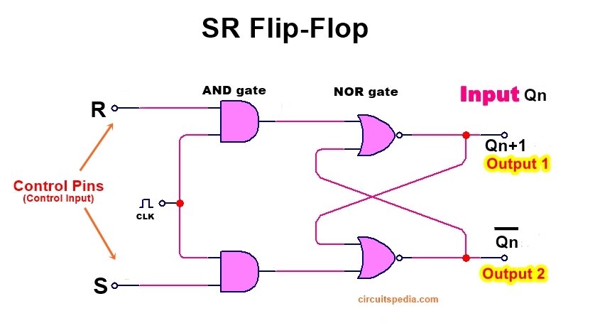
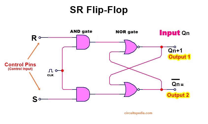
Input is given at the Qn and the output also gets on the same point Qn. But the output is denoted by Qn+1. 1 is actually the nth iteration of the cycle. Because FLIP-FLOP is a memory element and this stores data so the next iteration of the cycle is named Qn+1. Input and output are at the same point Qn. Qn Bar is the complement of Qn and for the valid operation of Flip-Flop, it should be a complement of Qn. complement means if Qn is 0 then the Qn bar is 1 and when Qn is 1 then the Qnbar is 0.
Here, we put the input at the point of Qn and output qn+1 also we get on the same point. R and S are also input pins, but really these are control pins. R means Reset, and s means Set. Both control pins are used to determine what mode we want the flip-flop to perform in flip-flop. R and S pins are used to control the mode of operation.
SR flip-flop using NOR gate
A simple one bit RS Flip Flops are made by using two cross-coupled NOR gates connected in the same configuration. The SR (set- reset) flip-flop is one of the simplest sequential circuits. The RS Flip Flop is considered one of the most basic sequential logic circuits.
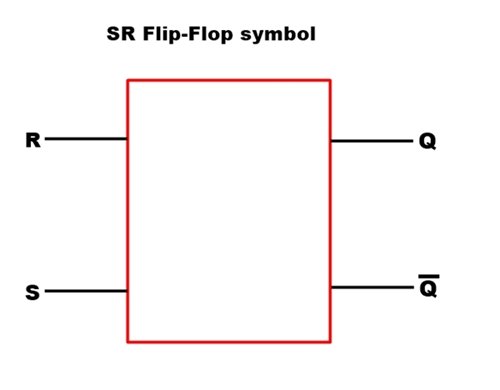
An SR flip-flop, also known as a set- reset flip-flop, is a basic type of flip-flop that has two inputs: “Set” (S) and “Reset” (R). It has two outputs, “Q” and “Q̅” (Q complement). The SR flip-flop can be in one of four possible states, determined by the input combinations. The output state changes based on the input values and the clock signal.
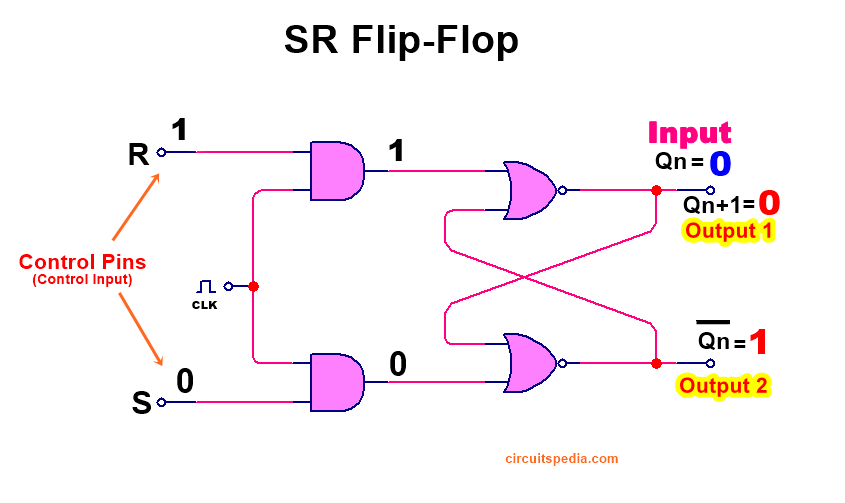
Now we make Reset pin 1 and take Qn is zero then functionality we see that output Qn+1 is zero.
If Qn is 1, then we see that output qn+1 is also zero. So we see that when the reset pin is 1, then the output is always zero whether the input at Qn is o or 1. In this mode flip flip-flop makes all input values reset, and it will not work as a memory element.
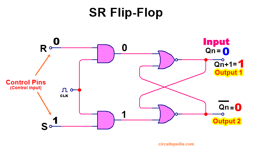
When the Set input pin is 1 and the Reset pin is zero, then we see the functionality. First, we check if the input value Qn is zero. The output is 1. And when take the input value at Qn is zero then the output is also 1 at Qn+1. So we see that when the set pin is 1 and the reset pin is 0 then the output will always be 1 in these cases.
Here, we use NOR gates to implement the R S Flip-flop circuit. implementation of R S flip-flop can be implemented using NAND gate.
When the clock value is zero and input at both R and S pin is zero, then, In this mode, the output is the same as the input value. R and S inputs can be connected directly, but the reason for the connection through the AND gate is to make Flip-Flop enable or disable. If the clock signal is high or 1 then the AND gate can give output High if any one of AND gate pin is high, in the Clock High or 1, the flip-Flop is in Enable condition but if the clk is LOW means flip-flop will disable because if even one input of AND gate is ) then the AND gate will give 0 output. So these inputs are called the control input pins.
Operation
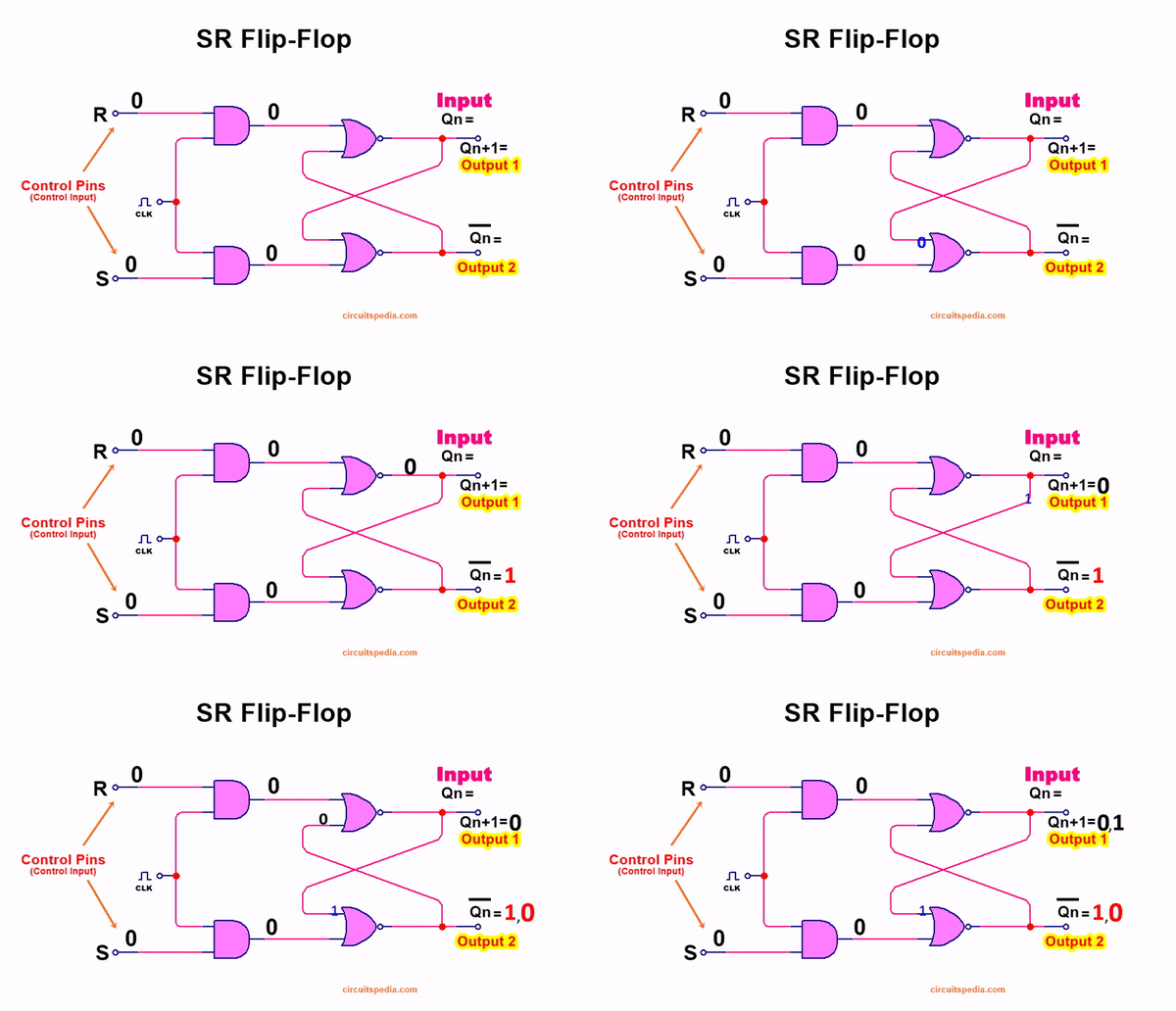
First condition: when R and S both are 0, Clk pin is High in the whole operation to enable. R and S both are 0, and clk is 1 so the AND gate will give 0. Now put Qn=0, this 0 goes to the NOR gate, and both pins of the NOR gate will be 0, so the output at Qn Bar is 1. This 1 is now going to the Upper NOR gate, and because one pin of this NOR gate is 0, the output will be 0. And this operation will be continued.
S=0, R=0, Qn=0, Qn+1=0
S=0, R=0, Qn=1, Qn+1= 1
Next condition-S(SET) is 0 and R (RESET) is 1. One AND gate gives output 1, and the second AND gate gives 0. Now, when Qn=0 we take. the 0 goes to the NOR gate and both pins is 0 of the NOR input gate will give 1 output at QnBar, This 1 goes to (upper) NOR gate, and here both inputs of NOR gate is 1 and this gives the output 0, and again this zero will go to Nor gate and give QnBar 1 and this process continuously operated.
S=0
R=1
Qn=0
Qn+1=0
S=0, R=1, Qn= 0, Qn+1= 0
S=0, R=1, Qn= 0, Qn+1= 1
S=1, R=0, Qn= 0, Qn+1= 1
In these operations, we see that when the RESET (R) pin is HIGH then the output Qn+1 is always LOW, and when the SET(S) pins are HIGH, the Output will always be HIGH.
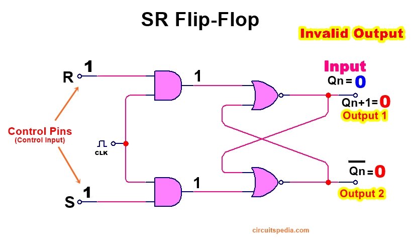
S=1, R=1, Qn= 0, Qn+1= 0
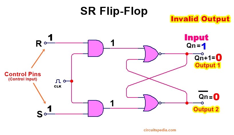
S=1, R=1, Qn= 1, Qn+1= 0
This is known as the running state of SR flip-flop because when both S and R pins are high, then the output will only be 0 and 0 even when Qn value 0 or 1 and not maintain the complementary with Qn and QnBar.
Truth Table of SR Flip-flop
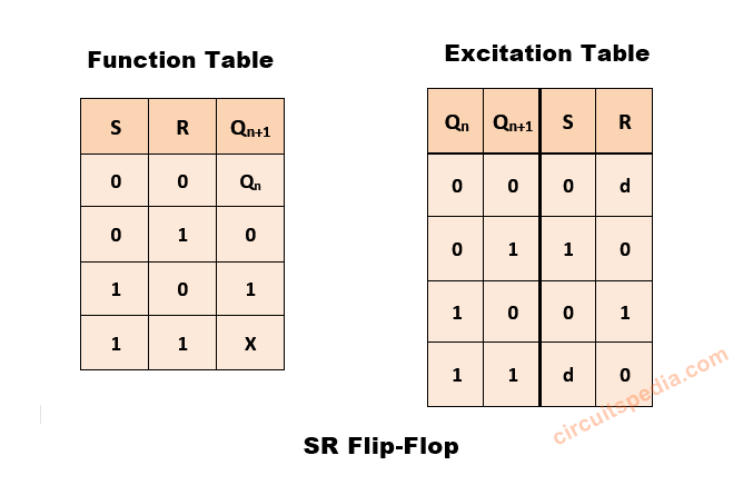
Function Table and Excitation Table of SR Flip-flop
R and S are actually the control pins that control the operation.
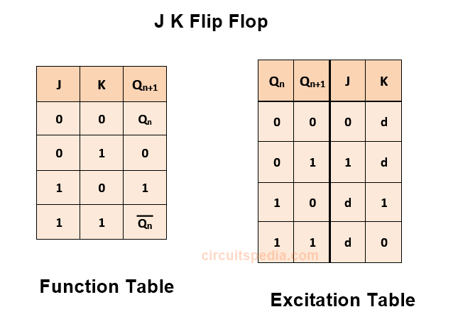
d means don’t care means either 0 or 1. Excitation means how we excite the Flip-flop for a required output state, Which logic input to be required to a particular output.
JK Flip-flop
Flop is named after Jack Kilby, an electrical engineer who invented IC. J-K Flip-Flop is a modified version of an S-R flip-flop. As we know that in SR flip-flop, there is an invalid state when both control inputs S and R are 1, and then the system was going to in a race condition. This problem is prevented and overcome in the J K Flip Flop. In this no “invalid” or “illegal” output state. The operation of the J_k Flip flop is the same as the RS flip flop.
A JK flip-flop is a type of flip-flop that has three inputs: “J” (set), “K” (reset), and a clock input. It can store one bit of information and has two outputs, “Q” and “Q̅” (Q complement). The JK flip-flop behaves similarly to the SR flip-flop but includes an additional feature to prevent invalid states.
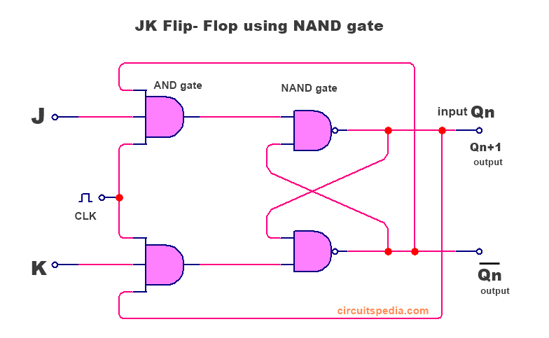
JK Flip flop diagram using NAND gate
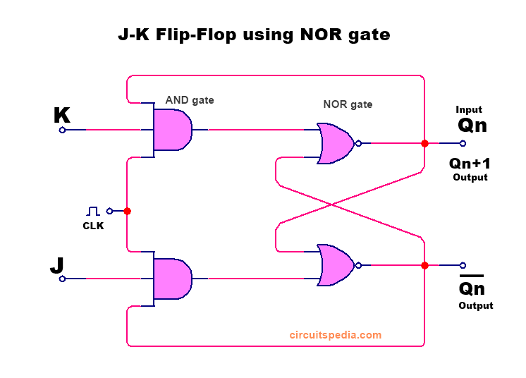
JK Flip-Flop using NOR gate
When S and R both pins are 1 then the output given by S R flip-flop is invalid, so resolving this problem some hardware circuit conversion made in implementation by using a feedback connection to the input of and gate from the output. After the changing of implementation, S and R will be named respectively J and K.
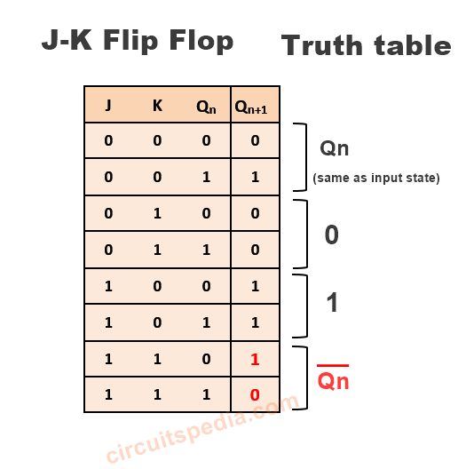
All functionality (except both R and S=1) of J K flip flop will same as R S flip flop means when we put the value of Qn= 1 and J and K = 0 then the output Qn+1=0
When J=0, K=1, and input given is 0, then the output at point Qn is Qn+1=0
And same as RS flip flop all values of output states are the same as RS Flip Flop.
But there was a problem when both R and S pins are 1. So we check here after putting the value Qn=0 . output Qn+1 at point Qn we get 1. And when Qn=1, the output value Qn+1 will be 0. We see that the value of the Qn and Q bar will complement each other means the system is not an invalid state or not in a running state.
JK flip-flop truth table
Function Table and Excitation Table
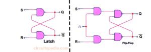
Latch– Latches are the basic building blocks using flip-flops are constructed. This has the capability to store 1 bit.
Clock signal
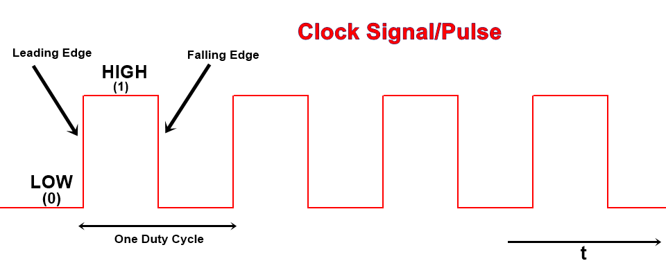 The clock signal repeated itself after every “t” second. A clock signal or clock pulse is a type of signal that oscillates between HIGH and LOW States continuously after a particular time delay. Digital circuits rely on clock signals to know when and how to execute the functions that are programmed
State changing in Flip-Flop occurred by the only clock signal.
If the output of a flip-flop is given by the 1st clock, this is denoted by Qn. But output given by the next clock is given by Qn+1
Short question and answers on Flip Flops
1. What is a Flip-Flop?
A flip-flop is a bistable multivibrator that has two stable states (0 and 1). It stores a single bit of data and is used in memory units, registers, and sequential circuits.
2. What are the different types of Flip-Flops?
The main types of flip-flops are:
SR (Set-Reset) Flip-Flop
D (Data or Delay) Flip-Flop
JK Flip-Flop
T (Toggle) Flip-Flop
Master-Slave Flip-Flop
3. What is an SR Flip-Flop?
An SR Flip-Flop (Set-Reset) has two inputs: Set (S) and Reset (R).
S = 1, R = 0 → Output = 1 (Set state)
S = 0, R = 1 → Output = 0 (Reset state)
S = 0, R = 0 → Output remains unchanged
S = 1, R = 1 → Invalid state (undefined behavior)
4. What is a D Flip-Flop?
A D Flip-Flop (Data or Delay Flip-Flop) captures the input data D at the clock pulse and stores it until the next clock cycle. It prevents invalid states found in SR Flip-Flops.
D = 1, Clock = 1 → Output = 1
D = 0, Clock = 1 → Output = 0
When Clock = 0, output remains unchanged.
5. What is a JK Flip-Flop?
A JK Flip-Flop is an improved version of the SR Flip-Flop that eliminates the S = 1, R = 1 invalid state.
J = 1, K = 0 → Set (Q = 1)
J = 0, K = 1 → Reset (Q = 0)
J = 0, K = 0 → No change
J = 1, K = 1 → Toggle (Q switches between 0 and 1)
6. What is a T Flip-Flop?
A T Flip-Flop (Toggle Flip-Flop) changes its state on every clock pulse if T = 1. It is useful for frequency division.
T = 0 → No change
T = 1 → Output toggles (0 → 1 or 1 → 0)
7. What is a Master-Slave Flip-Flop?
A Master-Slave Flip-Flop consists of two flip-flops connected in series to avoid race-around conditions.
The Master Flip-Flop captures input on the first clock edge.
The Slave Flip-Flop updates the output on the next clock edge.
8. What is the difference between Latch and Flip-Flop?
A latch is level-triggered, meaning it continuously updates output based on input when enabled. A flip-flop is edge-triggered, updating its output only at a specific clock transition.
9. What is a Clocked Flip-Flop?
A clocked flip-flop changes state only at specific clock pulses (rising or falling edges), making it synchronous with a timing signal.
10. What is the race-around condition in JK Flip-Flop?
The race-around condition occurs in a JK Flip-Flop when J = 1, K = 1, and the clock pulse is long. The output toggles rapidly, causing instability. This is solved using Master-Slave JK Flip-Flops.
11. How is a Flip-Flop used in Frequency Division?
A T Flip-Flop or JK Flip-Flop (J=K=1) divides the clock frequency by 2 at each stage. A series of flip-flops can achieve binary frequency division.
12. What are the applications of Flip-Flops?
Flip-Flops are used in:
✔ Registers & Memory Units
✔ Counters & Frequency Dividers
✔ Data Storage in Microprocessors
✔ Shift Registers for Data Transmission
✔ Control Circuits in Digital Systems
13. What is an Edge-Triggered Flip-Flop?
An Edge-Triggered Flip-Flop changes its state only on the rising edge or falling edge of the clock signal, avoiding race conditions.
14. How does a Flip-Flop store data?
A flip-flop stores 1-bit of data by maintaining its state until an input or clock signal changes it.
15. What is the difference between Positive Edge-Triggered and Negative Edge-Triggered Flip-Flops?
✔ Positive Edge-Triggered Flip-Flop: Activates on the rising edge of the clock pulse.
✔ Negative Edge-Triggered Flip-Flop: Activates on the falling edge of the clock pulse.
16. How does an SR flip-flop work?
An SR flip-flop operates based on its input combinations:
- When both S and R inputs are low (0), the flip-flop remains in its current state.
- When S is high (1) and R is low (0), the flip-flop is set, and the Q output becomes high (1).
- When R is high (1) and S is low (0), the flip-flop is reset, and the Q output becomes low (0).
- When both S and R inputs are high (1), it results in an invalid state, and the behavior is not predictable.
17. How does a JK flip-flop work?
A JK flip-flop operates based on its input combinations:
- When J and K are both low (0), the flip-flop remains in its current state.
- When J is high (1) and K is low (0), the flip-flop is set, and the Q output becomes high (1).
- When K is high (1) and J is low (0), the flip-flop is reset, and the Q output becomes low (0).
- When both J and K inputs are high (1), it toggles the output state. If Q is high, it becomes low, and vice versa.
18. What are the applications of SR and JK flip-flops?
SR and JK flip-flops have various applications, including:
- Memory elements: They can be used as basic storage units in registers and memory circuits.
- State machines: Flip-flops play a vital role in designing sequential circuits and state machines for control and data processing.
- Counters: Multiple flip-flops can be interconnected to form counters used for counting
Also Read.
-
Number system, Decimal, Binary, Octal, Hexa conversion
-
What is Opto-coupler/Opto-isolator
-
LOGIC GATES
-
Ohm’s Law

