LOGIC GATES
Logic gates are the basic building elements of any digital system or circuit. The name Logic gate is derived from the sense of the making decisions ability of such a device, and after making decisions it produces one output result. We can say that Logic gates are the fundamental building blocks of any digital circuits or digital systems.
There are 3 basic Types of Logic gates – (1)-AND, (2)-OR, (3)-NOT
Basically, Logic gates are elementary electronic logic circuit that can make a variety of different types of circuits by the interconnection of these three gates to perform complex logical operations of any computer. This is called logic design. Logic gates made a number of electronic devices and other digital components. In the practical application of logic gates, we see in the form of different Ics. These Ics are in LSI (Large scale integration), VLSI (Very-large-scale integration), and SSI (Small scale integration). Input and Outputs of Logic gates in only two levels called TRUE and FALSE, or HIGH and LOW, or ON and OFF, or very popular 0 and 1.
High (1 or TRUE or ON) means +5v
LOW(0 or FALSE or OFF) means 0v (or -ve supply)
This 2-level logic is also called Positive and Negative Logic.
AND GATE
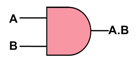
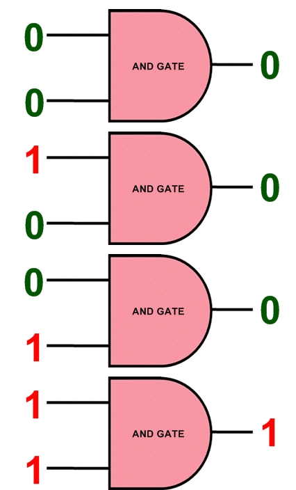
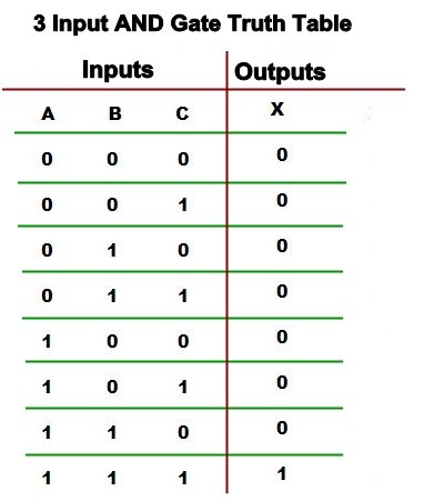
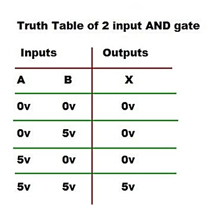
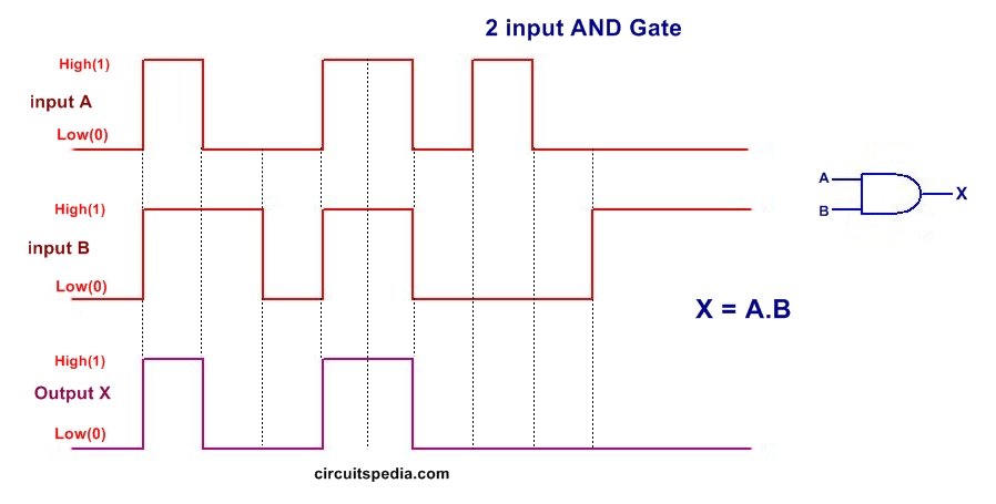
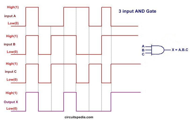
AND gate has two or more than two inputs and only one Output. In AND gate Output is High or 1 only when each input of it has in the HIGH state. Means output is 1 if only all inputs are at 1 level. If any of one input goes at 0 levels then the output of AND gate becomes 0.
Logic Symbol
Input Variables are represented by A, B, C…… and the output is written as X. In the Boolean expression, it can be written as X=A.B.C……. It can be read as X is equal to A and B and C ….or X is equal to A dot B dot C…. or X is equal to ABC…..
Truth table
3 input AND GATE Truth table
Realization of AND Gate-
AND gate may be realized by the use of diode and transistors. If it is made by using diodes then it is called DL(Diode Logic) and if using transistors it is called RTL (Resistor Transistor Logic).
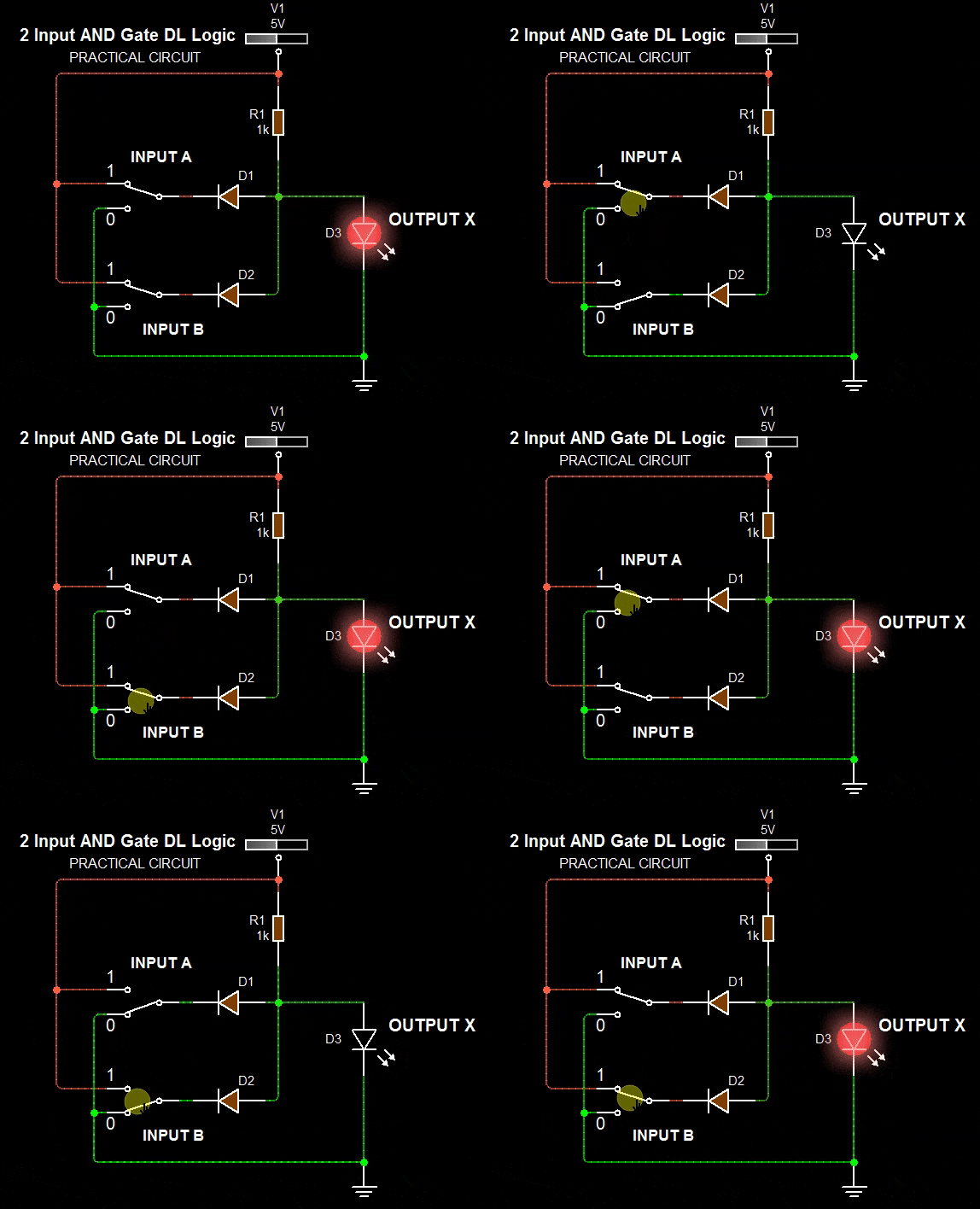
In the Diode Logic AND gate When the input A = +5v and input B is also +5v, in this case, both diodes D1 and D2 are off (because of reverse mode). And therefore no current flows through resistor R. So no voltage drop occurs across R and voltage remains at the output is HIGH.
Schematic diagram
When A=0, and B=0v or any one of A or B is 0v. Then both diodes or corresponding Diode D1 or D2 are ON and the circuit acts as a short circuit. In this condition the output X=LOW or 0v.
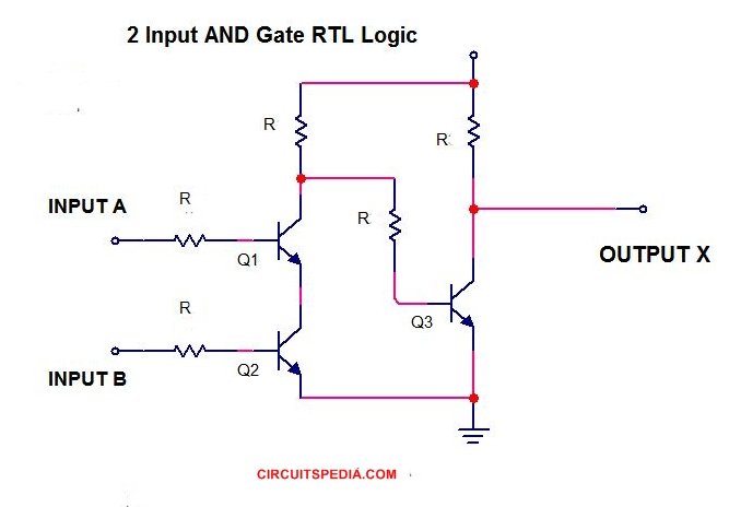
RTL AND Gate circuit
In the RTL AND gate or transistor gate, When A=0v and B=0v. Then the transistors Q1 and Q2 are off but transistor Q3 remains in ON, and the voltage at the output is LOW or 0v because of Q3 ON and current passes through Q3 and voltage is dropped through R.
If Anyone of input A or B is high then Either Q1 or Either Q2 will off and then no voltage drop occurs at R. So Q3 Will remain in turn on and therefore output will be LOW.
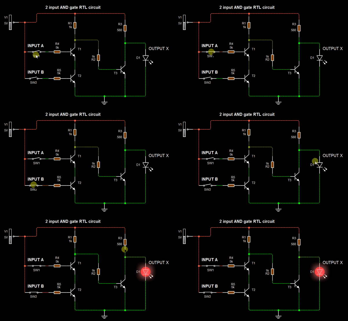
If input A and input B both are HIGH then both transistors Q1 and Q2 will turn on and the current passes through these transistors between ground and +5v and voltage will LOW at the collector pin of T1 and at the input of Q3 . So Q3 will off and no voltage drop at the collector pin and output will HIGH. At HIGH conditions the voltage at the output is approx 5v (X≈5v).
Practical Schematic diagram
The truth table of 2 input AND gate
OR gate
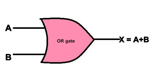
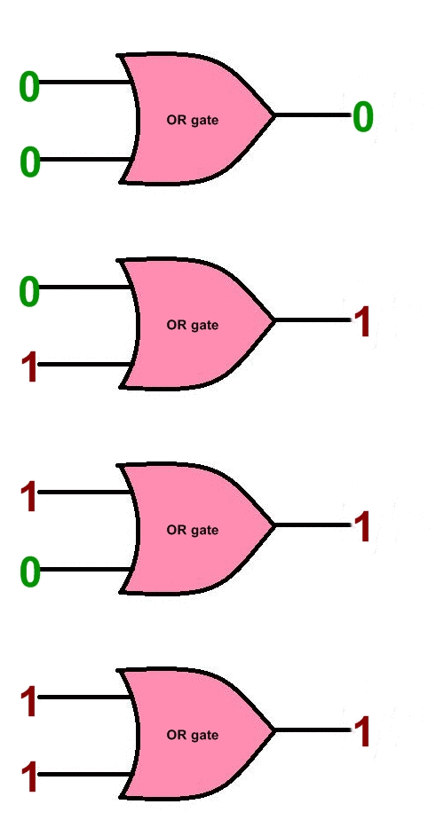
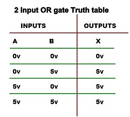
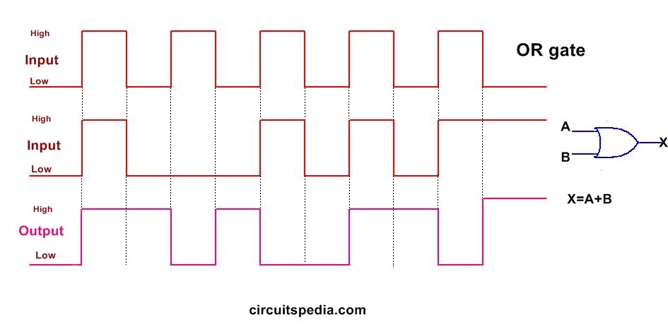
OR gate has also two or more two inputs but only one output. The output is HIGH or 1 if even any one of input is 1. The output is o or LOW if all of its input is in a LOW state or 0. OR gate is defined as the device whose output is o if any one of its inputs is 1.
Must read What is NOT gate
The Logic symbol for the OR gate is +. The Boolean expression for the output can be written as X=A+B+C+…… This is written as X is equal to A plus B plus C or it can also be read as X is equal to A or B or C or ……
OR GATE Truth table
The realization of OR gates can be made using Diodes(Diode Logic) or Transistors(RTL).
In the diode or gate, when both input A and B=0v or LOW, then both diodes D1 And D2 are OFF state because of reverse biasing. So No current pass Through R and No voltage drop will occur. Then the output X=0v. If both inputs or any one of both inputs is +5v. Then the corresponding diode D1 or D2 is On or both diode D1 and D2 are ON and a short circuit occurs across them. Therefore the output X is approx to +5v. voltage drop across diode is +5v-0.7v= 4.3v . But this is treated as HIGH or 1.
OR gate RTL circuit (Practical ckt)
In the Transistor (RTL) logic OR gate circuit, When both inputs A & B are 0v. Transistors Q1 and Q2 are OFF and Transistor Q3 is ON because of it gets Base voltage through Resistor R1. So the output voltage at the Collector pin of Q3 goes 0v by dropping of voltage with the ground at R2. If anyone of any input A or B is HIGH or 1 then the corresponding transistors in the ON state. So the voltage at the collector of that transistor goes to 0v by voltage drop and there is no Base voltage at the Q3 and no voltage drop occurs at R2, therefore, the output is HIGH OR 1.
The Universal Gates
Universal gates are defined as Which logic gates can implement any types of logic gates. There are two universal gates NAND and NOR. Both NAND and NOR gates can perform all the three basic logic functions of AND, OR, NOT. AOI (AND/OR/INVERT(NOT)) can be converted to NAND logic or NOR logic.
Types of Universal Gates
NAND Gate (NOT-AND)
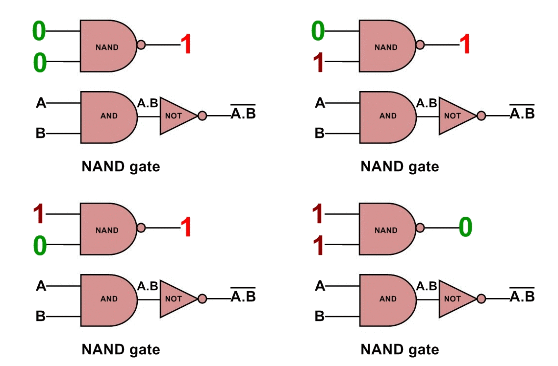
NAND gate is a combination of AND gate and NOT gate. If the output of AND gate is Inverted then it is called NAND gate. NAND = NOT AND. When AND output is NOTed or Inverted then it is called NAND gate.
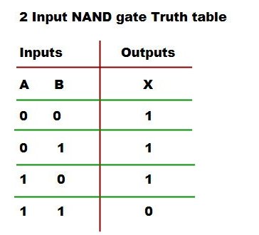
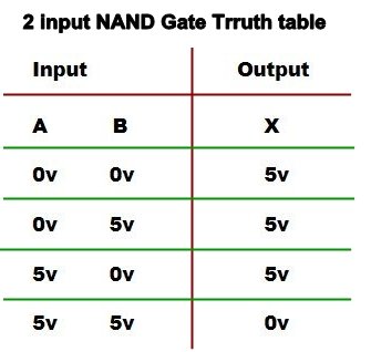
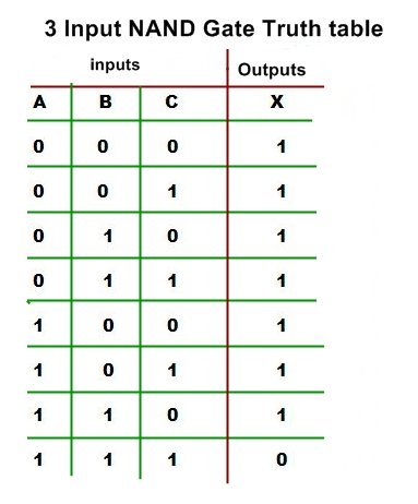
The output is 0 only if each input is 1 and output is 0 if anyone of any input or all inputs are 0. This means when all inputs are 1 then the output will 1 otherwise if different combinations of input the output is 0. The boolean expression of the NAND gate is written as
This is read as X=A.B.C….whole bar.
Realization of NAND gate-
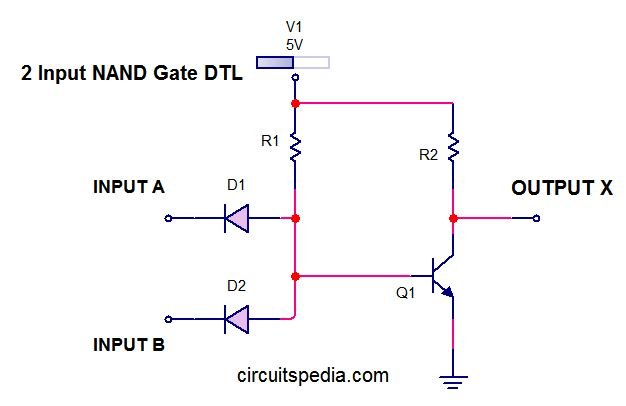
A two-input NAND gate can be realized using Diode Transistor Logic. When the input A and B both are HIGH or +5v then both diodes are off and the transistor gets base voltage through R1. So the transistor is ON and the output voltage at the collector is 0v because of the dropped voltage with the ground. When Both inputs A and B are 0v then both diodes are in ON because of forward bias (here 0v means negative supply). So the Base voltage of the transistor is 0v. So Transistor is in OFF and then the output is HIGH or approx +5v.
Schematic diagram
NAND GATE Truth table
NOR Gate
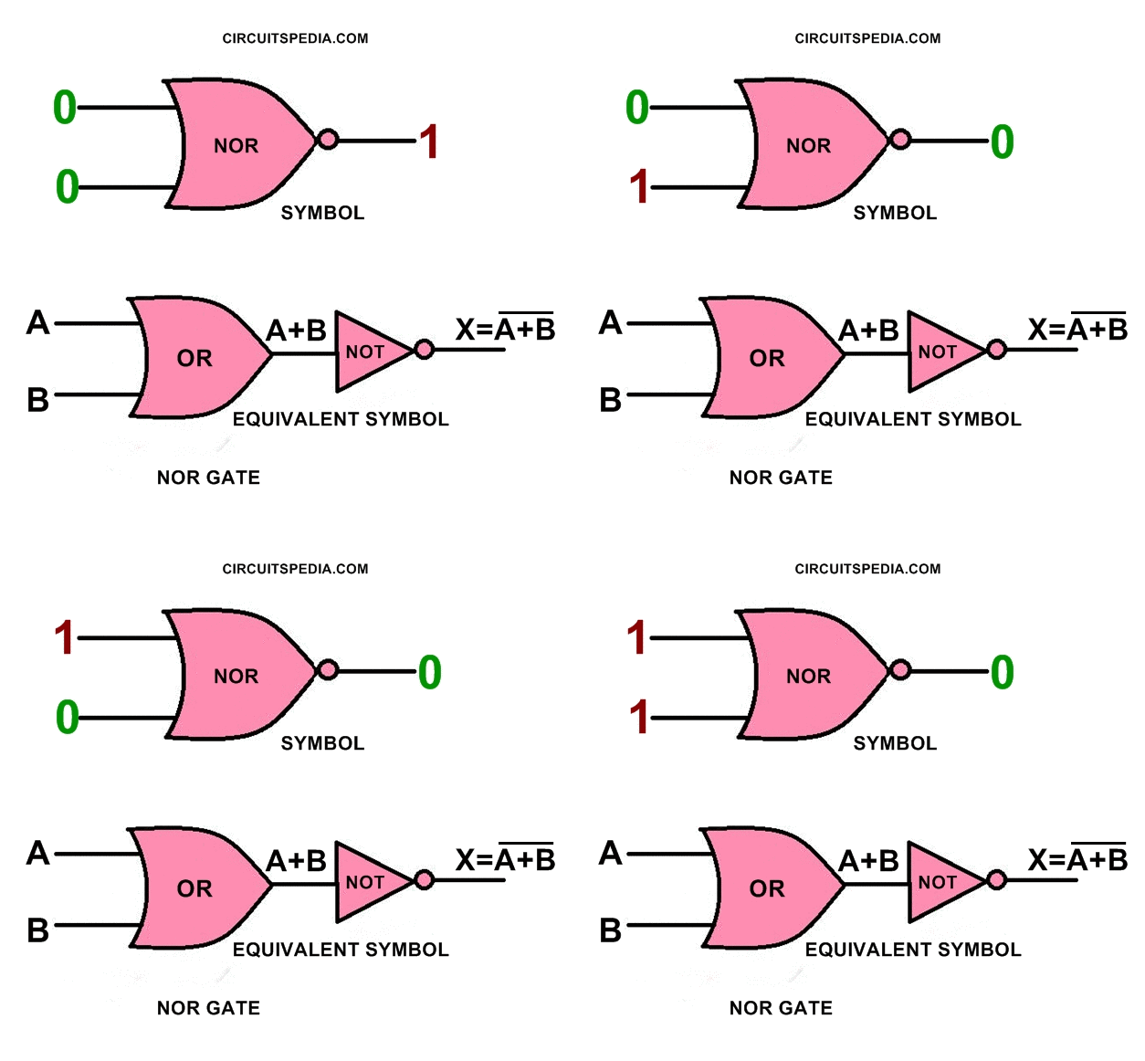
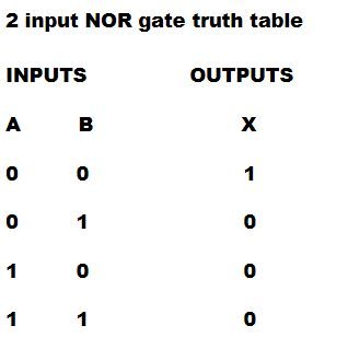
When the output of OR gate is NOTed or inverted then it is called the NOR gate. NOR means NOT OR. NOR gate is the combination of an OR gate and a NOT gate. The output is 1 or HIGH when only both input is 0 or LOW. Otherwise, the output is 0. The boolean expression for the NOR gate is expressed as given below This is read as X is equal to A plus B plus C plus …..whole bar.
NOR GateTruth table
Realization of NOR gate-
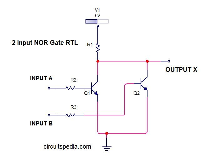
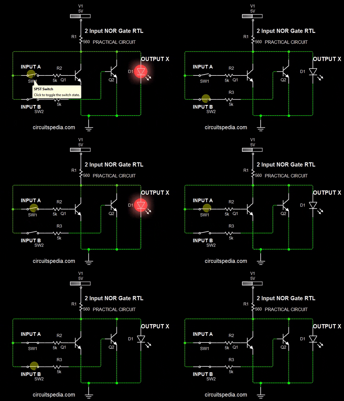
Two input RTL(Resistor transistor logic) NOT gate can be realized using two transistors and resistors. When Input A and B both are 0. A=0 and B=0. Then both transistors are OFF because no base voltage gets. So no current flows through transistors and no voltage drop occurs. Therefore only current passes through R the output is HIGH.
RTL NOR Gate Schematic diagram
Frequently asked questions (FAQ)
Q: What are logic gates? – Logic gates are electronic circuits that perform basic logical operations on one or more binary inputs to produce a binary output. They are the building blocks of digital circuits and computer systems.
Q: How many types of logic gates are there? – There are several types of logic gates, including AND, OR, NOT, NAND, NOR, XOR, and XNOR gates. Each gate has a specific function and truth table that determines its output based on the input(s).
Q: What is the AND gate?– The AND gate is a logic gate with two or more inputs and a single output. It produces a HIGH (1) output only when all of its inputs are HIGH; otherwise, it produces a LOW (0) output.
Q: What is the OR gate? – The OR gate is a logic gate with two or more inputs and a single output. It produces a HIGH output if at least one of its inputs is HIGH. The output is LOW only when all inputs are LOW.
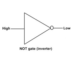
Q: What is the NOT gate? – The NOT gate, also known as an inverter, has a single input and a single output. It produces the logical complement of its input. If the input is HIGH, the output is LOW, and vice versa.
Q: What is the NAND gate? – The NAND gate is a combination of the AND gate followed by a NOT gate. It produces the complement of the AND gate’s output. The output of the NAND gate is LOW only when all inputs are HIGH.
Q: What is the NOR gate? – The NOR gate is a combination of the OR gate followed by a NOT gate. It produces the complement of the OR gate’s output. The output of the NOR gate is HIGH only when all inputs are LOW.
Q: What is the truth table for an OR gate?
A: An OR gate has two inputs (A and B) and one output (Y). The truth table for an OR gate is as follows:
A | B | Y
0 | 0 | 0
0 | 1 | 1
1 | 0 | 1
1 | 1 | 1
Q: What is the truth table for an AND gate?
A: An AND gate has two inputs (A and B) and one output (Y). The truth table for an AND gate is as follows:
A | B | Y
0 | 0 | 0
0 | 1 | 0
1 | 0 | 0
1 | 1 | 1
Q: What is the XOR gate? – The XOR (exclusive OR) gate is a logic gate with two inputs and a single output. It produces a HIGH output when the number of HIGH inputs is odd; otherwise, it produces a LOW output.
Q: What is the XNOR gate? – The XNOR (exclusive NOR) gate is a logic gate with two inputs and a single output. It produces a HIGH output when the number of HIGH inputs is even; otherwise, it produces a LOW output.
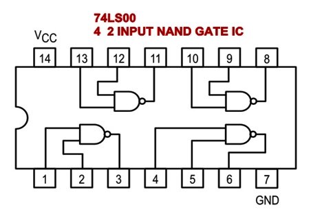
Q: Can logic gates have more than two inputs? – Yes, logic gates can have multiple inputs. AND, OR, NAND, and NOR gates can have any number of inputs. XOR and XNOR gates are typically limited to two inputs.
Q: Can logic gates have more than one output? -Generally, logic gates have a single output. However, certain specialized logic gates or integrated circuits may have multiple outputs, especially in complex digital systems.
Q: How are logic gates used? – Logic gates are used to manipulate and process binary information in digital circuits. They are the foundation of digital electronics and are used to design and build complex systems like computers, calculators, and electronic devices.
Q: Are logic gates only used in electronics? – While logic gates are primarily used in electronic circuits, their concepts and principles are also applicable in other fields, such as computer science, mathematics, and logic programming.
Q: Can logic gates be implemented using different technologies? – Yes, logic gates can be implemented using various technologies, including transistors, diodes, relays, optical devices, and even biological components in the emerging field of bioelectronics.
Q: Is there a limit to the number of logic gates that can be cascaded together? -There is no theoretical limit to the number of logic gates that can be cascaded in a digital circuit. However, practical limitations such as signal degradation
Also Read
-
How capacitor block dc current
-
What is Opto-coupler/Opto-isolator
-
Zener diode working
-
Dark Sensor Circuit










Great explanation of logic gates! I love how you broke down the functions of AND, OR, and NOR gates. It really helps clarify their roles in digital circuits. Looking forward to more posts on universal gates!
Great, do anyone mind merely reference back to it
It is actually a nice and helpful piece of information. I am happy that you just shared this useful information with us. Please keep us up to date like this. Thanks for sharing. rentacarkosovo
I am frequently to blogging we truly appreciate your content regularly. The content has really peaks my interest. I’m going to bookmark your blog and maintain checking choosing info.