4017 Counter ic
The 4017 IC is one of the most widely used decade counter integrated circuits (ICs) in digital electronics. It plays a crucial role in circuits that require sequential counting, LED chasers, and digital automation. This CMOS-based Johnson counter IC can be used to create fascinating lighting effects, counting applications, and automation projects, making it a go-to choice for electronics enthusiasts and engineers alike.
If you’re looking for an easy-to-use IC that helps with counting and sequencing operations, the 4017 Decade Counter IC is your answer. In this in-depth guide, we’ll explore its working principle, pin configuration, electrical specifications, and various real-world applications. Whether you’re a beginner in electronics or an advanced designer, understanding the 4017 IC will significantly enhance your projects.
What is the 4017 IC?
The 4017 IC is a decade counter/divider that can sequentially activate 10 different outputs (Q0 to Q9) in response to clock pulses. This means it can count from 0 to 9 and then restart from 0 automatically.
Due to its CMOS-based low-power design, it is highly efficient and can work with a wide range of input voltages (3V to 15V). The IC is widely used in counters, LED sequencing circuits, frequency dividers, and digital automation projects.
Unlike traditional binary counters, the 4017 IC provides individual decoded outputs, making it extremely useful for controlling multiple outputs sequentially without additional decoding circuitry.
This counter IC is also used in the electronic industries, medical electronic manufacturing devices, automotive industries, alarms and electronic instrumentation devices.
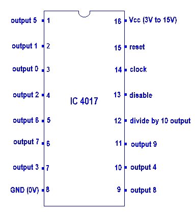
Pin diagram of 4017

 The 4017 IC has 16 pins, each serving a specific function. Below is a detailed description of its pin configuration:
| Pin Number | Pin Name | Function |
|---|---|---|
| 1 | Q5 | Output 5 (Sequential counting output) |
| 2 | Q1 | Output 1 |
| 3 | Q0 | Output 0 (First output in sequence) |
| 4 | Q2 | Output 2 |
| 5 | Q6 | Output 6 |
| 6 | Q7 | Output 7 |
| 7 | Q3 | Output 3 |
| 8 | GND | Ground (0V reference) |
| 9 | Q8 | Output 8 |
| 10 | Q4 | Output 4 |
| 11 | Q9 | Output 9 (Last output in sequence) |
| 12 | CO (Carry Out) | Used to cascade multiple ICs for extended counting |
| 13 | Clock Enable | Active HIGH; enables or disables counting |
| 14 | Clock Input | Receives the clock signal to trigger counting |
| 15 | Reset | Resets the count back to Q0 when HIGH |
| 16 | Vcc | Power supply input (3V – 15V) |
How Does the 4017 IC Work?
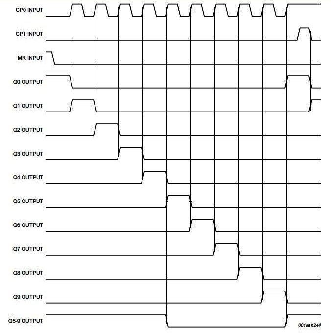
The 4017 IC operates as a sequential counter that advances its output each time it receives a clock pulse at Pin 14 (Clock Input). Here’s a step-by-step breakdown of how it works:
- Clock Signal Triggering: When a rising edge (low to high transition) of the clock pulse is detected at Pin 14, the IC advances to the next output.
- Sequential Activation of Outputs: Only one output (Q0 to Q9) is HIGH at any given time, and the sequence progresses with each clock pulse.
- Reset Function (Pin 15): When set HIGH, the IC immediately resets the count back to Q0 and stops further counting until it is set LOW again.
- Clock Enable (Pin 13): If this pin is set HIGH, the clock signal is ignored, and the IC stops counting. Setting it LOW allows normal operation.
- Carry Out (Pin 12): This pin outputs a signal after every 10th clock pulse, making it useful for cascading multiple 4017 ICs for extended counting.
Example of Sequential Counting
If an LED is connected to each output (Q0 to Q9), the LEDs will turn on sequentially as the clock pulses arrive. This effect is widely used in LED chasers, running lights, and digital counters.

Technical Specifications of the 4017 IC
- Operating Voltage: 3V – 15V (Typically 5V or 12V)
- Maximum Clock Frequency: 5 MHz (Higher frequencies may cause instability)
- Output Current Per Pin: 10mA (Direct LED driving possible with resistors)
- Total Outputs: 10 (Q0 to Q9)
- Reset and Clock Enable Inputs: Active HIGH
- Power Consumption: Low (Thanks to CMOS technology)
- Package Types: DIP-16, SOP-16
Applications of the 4017 IC
The 4017 IC is a favorite among electronics designers due to its simplicity and versatility. Here are some of its most popular applications:
1. LED Chaser Circuits
One of the most common uses of the 4017 IC is in LED chaser circuits. By connecting LEDs to Q0 – Q9, the LEDs light up sequentially, creating a stunning visual effect. This application is widely used in advertising boards, decorative lighting, and entertainment setups.
2. Digital Counters & Event Counters
The 4017 IC is frequently used in digital counters, where it helps count pulses and triggers a specific output after a set number of pulses. These are commonly used in production counters, scoreboards, and event tracking systems.
3. Frequency Divider Circuits
By setting the Reset pin (Pin 15) at specific counts, the 4017 IC can act as a frequency divider. This is useful in timer circuits, frequency multipliers, and pulse-generating circuits.
4. Traffic Light Controller
The IC is often used in traffic light controllers, where it sequences signals to control different traffic phases automatically.
5. Music & Light Synchronization
In sound-activated LED projects, the 4017 IC can be synchronized with audio signals to create light effects that match the rhythm of the music.
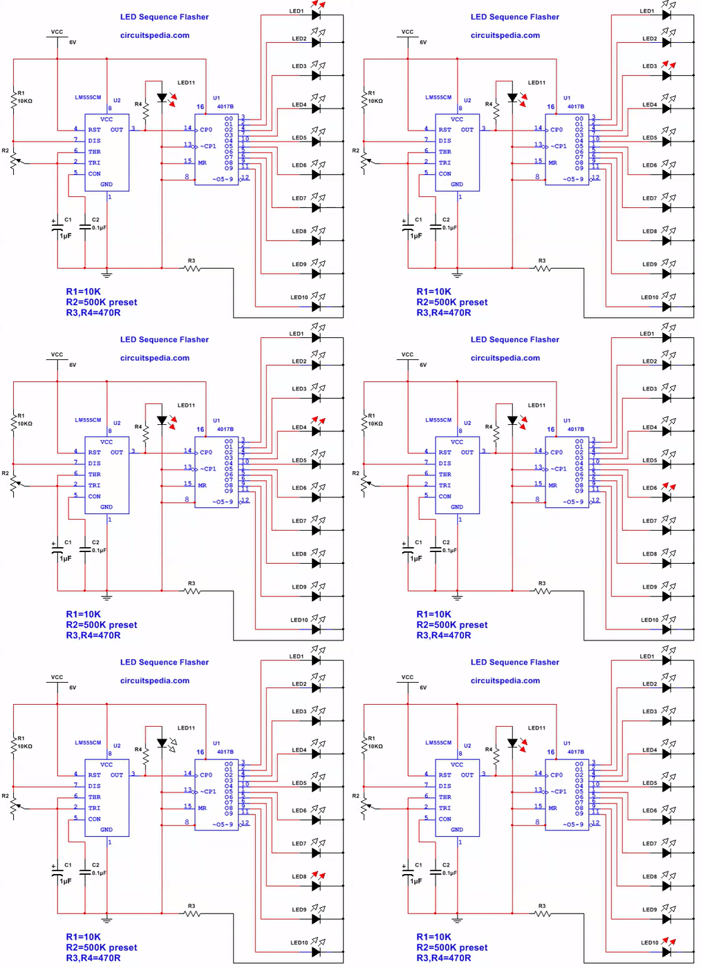
One of the best and simplest applications of this 4017 counter IC is the LED Flasher in Sequence.
This is the circuit diagram of the LED flasher using 4017. When the clock pulses get at the input pin, all 10 outputs are High (ON) one by one according to the pulse speed at the input pin. At pin 14 Input clock pulse is provided using the 555 timer ic. At each positive clock pulse, the output shifts to the next output pin, and the previous output is off accordingly. The animated schematic diagram below shows how it works. This is the simulation of the counter circuit using the led as output detection.
How to use 4017 IC in LED chaser circuits
- The supply voltage of this IC is 3V to 15V.
- It is compatible with TTL (Transistor-Transistor Logic).
- The clock speed or operational speed of the CD4017 IC is 5 MHz.
Touch on-off Switch using 4017
Operational amplifier (Op-amp)


Hi; I really like your explanation of the CD4017 Decade/Counter. I’m from Canada, and I’m reaaly interested in anything electronics. I’m actually tr4ying to gather informations on a project for my son.He’s building a flying eagle logo sign and want me to install some flashing white leds in sequence. He will need around 100-150 leds. I am thinking of using a 555 timer and some CD4017, and I’m wondering if it is possible to use more than 1 CD4017, since I’ll be using 100-150 leds. Or, is there a simpler way I could do it ??. I would really appreciate if you could give me some advices. Thank you very much.
Maurice Petit