PIN diode
What is PIN diode
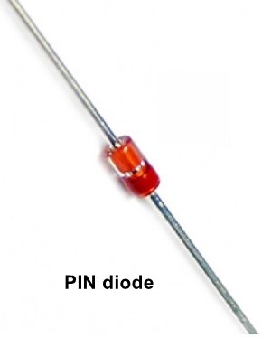
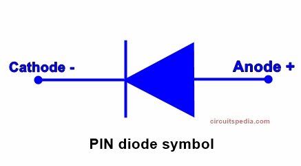
The name “PIN diode” derives from its three-layer structure: P-type, Intrinsic, and N-type. The P and N layers are heavily doped, while the Intrinsic layer remains undoped. This arrangement forms a PIN junction, enabling the diode to exhibit distinct characteristics.
A PIN diode is one type of diode in which a wide undoped (pure form), intrinsic semiconductor region placed between (sandwiched) a P-type and N-type semiconductor region. This intrinsic semiconductor layer has high resistivity. The high resistive layer of the intrinsic region provides a large electric field between the P and N-region. It differs from a normal diode in the sense that it has an extra layer in between the p and the n junctions. The P and N-Type is heavily dopped and this is used for contacting terminals but the middle layer is in a pure crystal of silicon or germanium and this layer behaves like an insulator and does not conduct current well.
The PIN diode was first used in the year 1952 as a low-frequency and high-power rectifier. In any PN junction, the P region contains holes as it has been doped to ensure that it has a predominance of holes. Similarly, the N region has been doped to contain an excess of electrons. The intrinsic region between the P and N contains no charge carriers as any holes or electrons combine. As the depletion region has no charge carriers, it acts as an insulator. The depletion layer exists within the PIN diode, but when we connect in forward bias, then both types of carriers come into the depletion layer and together make to start the current conduction. By this property of PIN diode, we can say that pn junction and PIN diode are the same, but there is one difference is it has one extra layer between p and n.
The i-region has high resistance, which obstructs the flow of electrons to pass through it. PIN diode is not suitable for rectifier applications. The occurrence of an intrinsic layer can significantly increase the breakdown voltage for the application of high-voltage.
PIN diode working
When the diode is connected in a forward biased, the charges are continuously injected into the I-region from the P and N-region. This reduces the forward resistance of the diode, and then it behaves like a variable resistance. The charge carriers do not immediately combine to the Intrinsic layer from the P and N layers. A quantity of charge stored in the intrinsic layer decreases their resistivity as the applied current.
When forward-biased, it acts like a current-controlled variable resistance.
The quantity of the charges stored in the intrinsic Layer/region depends on their recombination time. The forward current starts flowing into the I region.
Where, Q be the quantity of charge stored in the depletion region
IF – forward current
τ- recombination time
The resistance (Rs) of the current under forwarding biased is inversely proportional to the charge Q stored in the intrinsic region.
From equation (1) and (2), we ge
Where, w – width region
μ – electron mobility
μ0 – hole mobility
The above equation shows that the resistance of the intrinsic region depends on the width of the region.
In reverse bias, the diode behaves like a capacitor and the P and N Layers act like the positive and negative plates of the capacitor, and the intrinsic region is the insulator material between the plates.
When the diode is connected in reverse bias, the width of the depletion Layer/region increases, and the thickness of the region also increases until the entire mobile charge carrier of the I-region is swept away from it. The reverse voltage required for removing the complete charge carrier from the I-region is known as the swept voltage.
Where, A – junction diode
w – intrinsic region thickness
The lowest frequency at which the effect starts to begins is expressed as
Where, ε – silicon dielectric constant
Structure of PIN diode
As per the name of this diode, the PIN diode has three layers
- P-type Layer
- I (Intrinsic) Layer
- N-type Layer
The intrinsic layer makes this diode different as compared with the normal PN junction diode. PIN diode has three layers, whereas PN junction diode has only two layers.
When forward biased, a PIN diode allows current flow through the diode due to the reduced depletion region width in the Intrinsic layer. Conversely, when reverse-biased, the depletion region expands, limiting the flow of current. This property enables PIN diodes to be used as fast-switching devices.
Features of a PIN diode
PIN diodes possess several notable features that make them highly advantageous for numerous applications:
a) Fast Switching Speed: The intrinsic region’s wide area, combined with the reduced depletion region during forward bias, enables PIN diodes to switch rapidly. This capability is crucial in applications where quick response times are necessary.
b) Low Noise and High Sensitivity: The Intrinsic layer’s high resistivity minimizes the recombination of charge carriers, making PIN diodes ideal for applications requiring low noise levels and high sensitivity, such as photodetection and signal control.
c) High Power Handling: PIN diodes can handle relatively high power levels due to their robust construction and wide junction area. This characteristic is particularly advantageous in RF applications, where power-handling capability is essential.
Application of PIN diode
- As a High Voltage Rectifier– The large width of the intrinsic layer allows the ability to the diode to tolerate high reverse voltage without the breakdown of the diode. Thus, rectification at high voltage can be implemented with a PIN diode. S0: This diode is used as a high-voltage rectifier.
- As Radio and Microwave frequency Switch, The PIN diode makes an ideal RF switch. in this case, the diode operated in reverse biased, when the diode is reversed bias. The level of isolation is increased. Due to the intrinsic layer between the PN junctions, the level of capacitance does Not store any charge and immediately changes from conduction to insulation and vice versa.
- As an Attenuator and RF protection Circuit–It is mainly useful for RF design applications and also for providing the switching, or an attenuating element in RF attenuators and RF switches.
- As Photodiode– The PIN diode is used for converting light energy into electrical energy. When the light falls on the depletion region, a small current is produced. IN PIN diode there are wide depletion region so, wide are of depletion region gets more volume of light to produce current and changes occur according to light easily
Advantages of PIN diode
- High reverse breakdown voltage– The PIN diode can be used as a high-voltage rectifier. The wider intrinsic region provides greater isolation between the PN and N regions, allowing higher reverse voltages to be tolerated.
- High Capacitance– The width of the intrinsic layer is large due to which the capacitance of the diode is low. As the capacitance of a device is inversely proportional to the intrinsic region thickness.
- RF and Microwave Switching
- Suitable for High frequency– At higher frequencies, PIN diode acts as a resistor. The charges stored in the intrinsic region. At small frequencies, the charge can be separated and the diode switched OFF.
- Power Limiters and Protection Circuits– The high power-handling capability of PIN diodes allows them to be used as power limiters, protecting sensitive components from excessive power levels in RF systems.
- RF Phase Shifters – PIN diodes can alter the phase of RF signals, making them valuable components in phased array antennas, beamforming systems, and frequency synthesizers
- Attenuators and RF Modulators/Demodulators – PIN diodes are employed in attenuators to control signal strength in RF circuits. Additionally, they serve as RF modulators and demodulators, enabling the conversion of RF signals to analog or digital formats.


