- Bipolar (BJT) Single Transistor, NPN, 80V, 1.5A, 12.5W, TO-126, Through Hole
BD139 is the medium power NPN bipolar junction transistor. The BD139 is a commonly used NPN power transistor designed for audio, switching, and amplifier applications. It has max output current load capacity across collector to emitter upto 1.5A
Specifications of BD139
- Type: NPN
- Maximum Collector-Emitter Voltage (Vceo): 80V
- Maximum Collector-Base Voltage (Vcbo): 100V
- Maximum Emitter-Base Voltage (Vebo): 5V
- Maximum Collector Current (Ic): 1.5A
- Maximum Power Dissipation (Ptot): 12.5W
- DC Current Gain (hFE): 25 to 250 (depending on the operating current)
- Package: TO-126
Collector -Emitter Voltage VCEO
BD135: 45V
BD137: 60V
BD139: 80V
Collector Current IC : 1.5A
Collector Peak Current ICM : 2.0 A
Features of BD139 transistor
- High Voltage Capability: Can handle up to 80V between the collector and emitter.
- Moderate Current Handling: Can switch or amplify currents up to 1.5A.
- Low Saturation Voltage: Ensures efficient operation with low power loss.
- Thermal Stability: The package allows for better heat dissipation compared to smaller transistors.
- High Gain: Suitable for various amplification tasks due to its high DC current gain.
- Audio Amplifiers:
-
- Used in the output stages of audio power amplifiers where moderate power and good linearity are required.
- Switching Applications:
-
- Commonly used in circuits for switching loads, such as motors, relays, and LEDs, due to its ability to handle relatively high currents and voltages.
- Voltage Regulators:
-
- Plays a role in maintaining a stable voltage in power supply circuits, often used in conjunction with other components.
- Driver Stages:
-
- Utilized in driving higher power transistors in larger circuits, serving as an intermediary stage to boost current capacity.
- General-Purpose Applications:
-
- Suitable for a wide range of electronic circuits, including signal amplification, oscillators, and other medium-power applications.
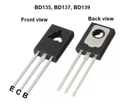
Pin Configuration:
- Collector (C): Connected to the load or the positive voltage supply in a typical circuit.
- Base (B): The control terminal, which modulates the flow of current between the collector and emitter.
- Emitter (E): Typically connected to the ground or the negative supply voltage.
Practical Tips for Using the BD139
- Heat Management: Use a proper heatsink if operating near the maximum power dissipation to prevent thermal damage.
- Base Resistor: Use a base resistor to limit the base current and protect the transistor from excessive current.
- Circuit Design: Check the hFE range to ensure the transistor matches the required gain for your circuit.
The BD139 is a versatile transistor widely used in electronics due to its robustness and reliable performance across a range of applications.
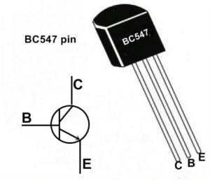
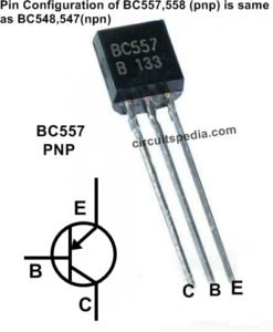
Complementary BD136, BD138, BD140 (PNP) are recommended with BD135, BD137, BD139
Equivalent – BD230(ECB), BD233(ECB), TIP31C(BCE) etc
Download Datasheet Pdf
-
bd135_bd137_bd139 (CDIL) –Download
-
bd135_bd137_bd139 (Motorola)– Download
-
BD139-Datasheer (ON Semiconductor) –Download
-
BD135 (Philips) –Download
bd135_bd137_bd139 datasheet (CDIL)
BD139-Datasheer (ON Semiconductor)
bd135_bd137_bd139 (Motorola)
BD135 -BD139 datasheet (Philips)

