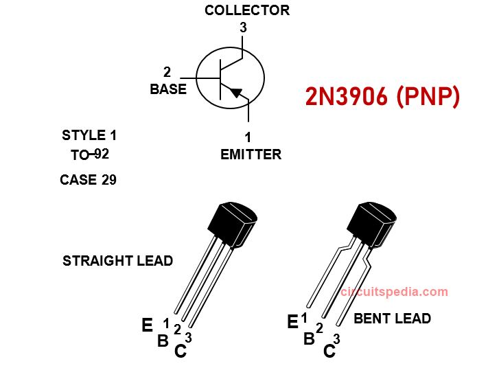
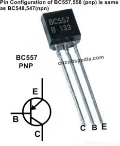
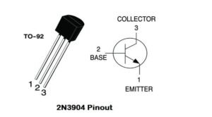
The 2N3906 is a widely used Low Voltage and low current PNP bipolar junction transistor (BJT). This transistor is mainly used in low-power high-speed switching applications. Maximum Collector current capacity for output load is 200ma. This transistor is much similar to BC557 or BC558 transistor, gain and max voltage rating (Emitter to collector voltage) is lower than BC557. This transistor is Well Suitable for TV And Home Appliance Equipment, Small Load, high-speed switching in industrial applications. 2N3904 is the NPN complementary of this.
- Type: PNP BJT
2N3906 Maximum Ratings
- Collector-Emitter Voltage (-Vceo): 40V
- Collector-Base Voltage (-Vcbo): 40V
- Emitter-Base Voltage (-Vebo): 5V
- Collector Current (-Ic): 200mA
- Power Dissipation: 625 mW
- Operating and Storage Junction Temperature Range TJ, Tstg = −55 to +150 °C
- Transition Frequency (ft): 250 MHz
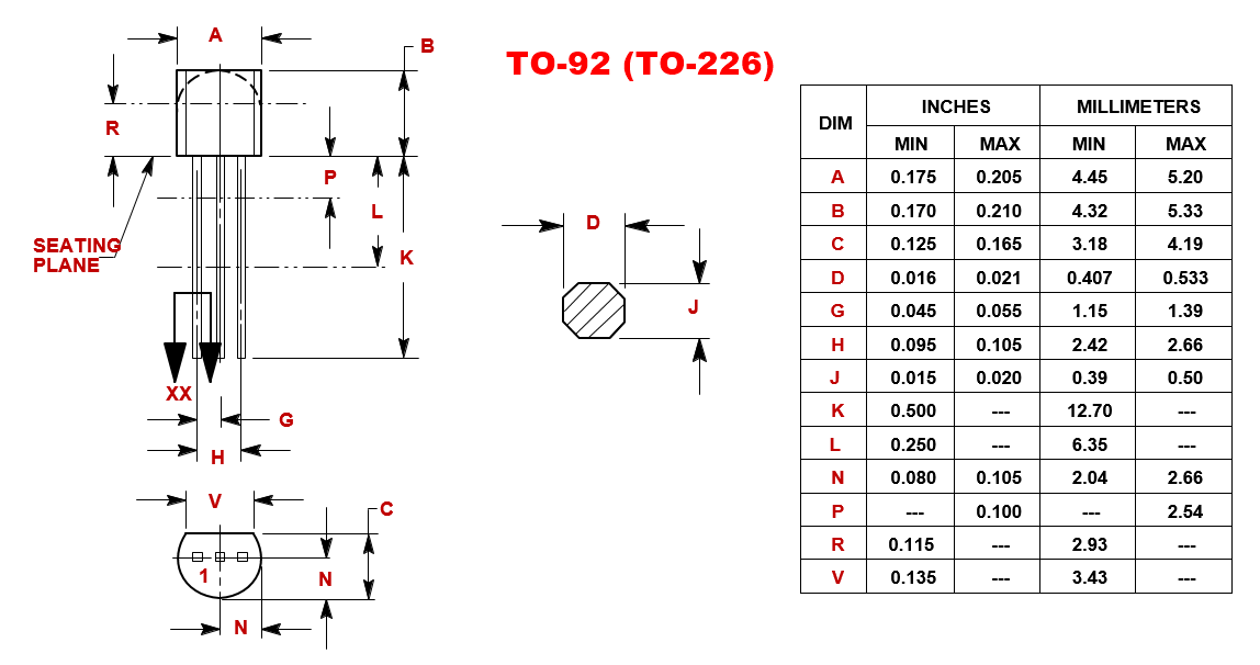
- Package: TO-92
- Gain (hFE): Typically ranges from 100 to 300
Applications of 2N3906 Transistor
- Switching Applications: The 2N3906 can be used to switch low power devices, making it suitable for signal switching.
- Amplification: It can amplify low power audio or other signals in electronic circuits.
- Analog Circuits: It is used in various analog circuits such as oscillators, signal generators, and voltage regulators.
- Complementary Pair: Often used in conjunction with its NPN counterpart, the 2N3904, in push-pull amplifier configurations.
- Oscillators- in creating clock signals, generating tones, and other applications requiring a stable periodic signal.
Equivalent or alternate options of 2N3906
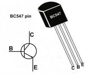
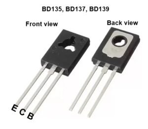
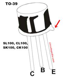
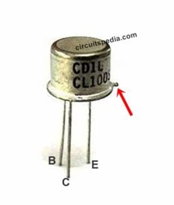
BC557(pin CBE), BC558(pin CBE), BD136(pin ECB), BD138(pin ECB), BD140(pin ECB), SK100
Working Principle
Basic Operation
The 2N3906 is a PNP transistor so being a PNP transistor it operates when a small current flows from the emitter (E) to the base (B), allowing a larger current to flow from the emitter to the collector (C). working of 3906 transistor jin different modes:
- Cutoff Mode: In this mode, the transistor is off. There is no base current (IB), and hence, no collector current (IC). The voltage between the base and emitter (Vbe) is not sufficient to forward bias the base-emitter junction.
- Active Mode: In this mode, the transistor acts as an amplifier. A small current flowing into the base-emitter junction controls a larger current flowing from the emitter to the collector. The base-emitter junction is forward-biased (Vbe is typically around -0.7V), and the base-collector junction is reverse-biased.
- Saturation Mode: In this mode, the transistor is fully on. Both the base-emitter and base-collector junctions are forward-biased. The transistor allows maximum current to flow from the emitter to the collector. This mode is used for switching applications where the transistor acts like a closed switch.
Biasing
Because this is a PNP transistor. The proper biasing of this transistor should as following.
- The emitter is connected to a positive voltage.
- The base is connected to a voltage that is less positive than the emitter.
- The collector is connected to a voltage that is more negative than the base.
Switching Application
In a typical switching application:
- The emitter is connected to the positive supply voltage.
- The collector is connected to the load (e.g., an LED) and then to ground.
- A resistor is placed between the base and ground to control the base current.
When a positive voltage is applied to the base, the base-emitter junction becomes forward-biased, and the transistor turns on, allowing current to flow from the emitter to the collector, thus powering the load.
Amplification Application
In an amplification setup:
- The emitter is connected to the positive voltage supply through a resistor.
- The base is connected to the input signal through a coupling capacitor.
- The collector is connected to the load and then to the ground.
The small input signal at the base controls the larger current flow from the emitter to the collector, resulting in an amplified output signal.
Datasheet 2N3906 (ON semiconductor)
Datasheet 2N3906 (ST)
Datasheet 2N3906 (Diodes Incorporated)

