The 2N3904 transistor is a versatile and widely used component in electronic circuits for switching and amplification. The maximum output current across collector to emitter is 200mA , means we can not connect load that required current more than of 200ma. The 2N3904 is a widely used NPN bipolar junction transistor (BJT) suitable for general-purpose low-power applications. The PNP complementary pair of this transistor is 2N3906.
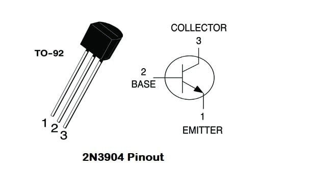
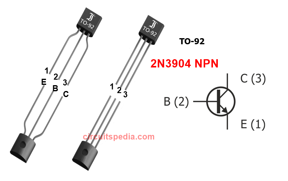
The 2N3904 transistor typically comes in a TO-92 package with three pins
Equivalent or alternative of 2N3904
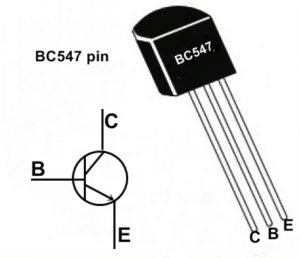
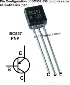
BC548, BC549, BC546(Pin CBE), 2N2222 (Pin EBC)
Pin Configuration
- Collector (C)
- Base (B)
- Emitter (E)
Material of Transistor: Si
Polarity: NPN
- Maximum Collector-Base Voltage (Vcb): 60 V
- Maximum Collector-Emitter Voltage (Vce): 40 V
- Maximum Emitter-Base Voltage (Veb): 6 V
- Maximum Collector Current Ic max: 200m A
- Max. Operating Junction Temperature (Tj): 135 °C
- Transition Frequency (ft): 300 MHz
- Collector Capacitance (Cc): 4 pF
- Forward Current Transfer Ratio (hFE), Max : approx 200
- Package: TO-92
Uses of 2N3904
- Switching Applications: The 2N3904 can be used to switch low-power devices on and off- In a switching circuit:
- The emitter is connected to ground.
- The collector is connected to the load (e.g., an LED) and then to the positive voltage supply.
- A resistor is placed between the base and a control signal to limit the base current.
When a positive voltage is applied to the base, it forward-biases the base-emitter junction, turning on the transistor and allowing current to flow through the load.
- Amplification: It can amplify low-power audio or other signals in electronic circuits- In an amplifier circuit:
- The emitter is connected to ground through a resistor.
- The base is connected to the input signal through a coupling capacitor.
- The collector is connected to the positive voltage supply through a load resistor.
- Analog Circuits: Used in oscillators, signal generators, and voltage regulators.
- Complementary Pair: Often used with its PNP counterpart, the 2N3906, in push-pull amplifier configurations.
Working Principle of 2N3904 transistor
The 2N3904, being an NPN transistor, operates by controlling the current flow through its collector-emitter path with the current applied to its base-emitter junction. Here’s a breakdown of its operation in different modes:
Cutoff Mode
- Condition: No base current (IB) flows.
- Effect: The transistor is off, and no current flows from the collector to the emitter (IC = 0).
Active Mode
- Condition: The base-emitter junction is forward-biased (Vbe ≈ 0.7V), and the base-collector junction is reverse-biased.
- Effect: A small base current controls a larger collector current. The transistor can amplify the input signal.
Saturation Mode
- Condition: Both the base-emitter and base-collector junctions are forward-biased.
- Effect: The transistor is fully on, and maximum current flows from the collector to the emitter. This mode is typically used for switching.
Biasing
For an NPN transistor like the 2N3904
- The emitter is connected to ground.
- The base must be at a higher voltage than the emitter for the transistor to turn on.
- The collector is connected to a positive voltage supply through a load.
In a switching circuit:
- The emitter is connected to ground.
- The collector is connected to the load (e.g., an LED) and then to the positive voltage supply.
- A resistor is placed between the base and a control signal to limit the base current.
When a positive voltage is applied to the base, it forward-biases the base-emitter junction, turning on the transistor and allowing current to flow through the load.
In an amplifier circuit:
- The emitter is connected to ground through a resistor.
- The base is connected to the input signal through a coupling capacitor.
- The collector is connected to the positive voltage supply through a load resistor.
The input signal at the base modulates the current flow from the collector to the emitter, resulting in an amplified output signal.
2n3904 datasheet (809kb)



I respect your piece of work, appreciate it for all the informative posts.