4017 Counter ic Working
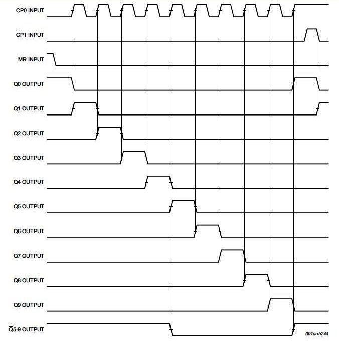
CD4017 or HCF4017BE or 74HC4017 is a CMOS decade counter/ Divider. It has 16 pins and this counter has 10 decoded outputs. This is known also as the 10 stages ‘Johnson decade counter. It has a total of 10 outputs. when a clock signal from the clock input is given the output turns to Highl one by one in sequence. When the clock input is given to input, at each pulse of the clock input signal the output turns on in sequence.
CD4017 is the most popular ic which is widely used in various applications like Binary counter, Decoder, Decade counter, Frequency division, etc. This is more useful in different types of projects like Light Chaser, Remote controlled Switches, Alarms, Touch ON-OFF switches, Clap switches, Matrix Die, etc.
This counter IC is also used in the electronic industries, medical electronic manufacturing devices, automotive industries, alarms and electronic instrumentation devices.
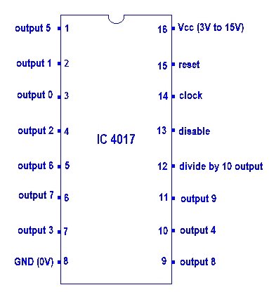
Pin diagram of 4017
Clock pin (pin14)- This is the input pin of this counter ic which gets the input clock signal from the external circuit. Whenever pin 14 get a clock pulse or it goes high to Low, it provides the output. At the first clock pulse pin 3 will turn high and give output; for the next pulse pin 2 will be high and provide output and after from pin 4 and so on. After 10 pulses it will repeat and again start to give output from Q0.
Reset pin (pin 15) – This pin is known as a reset pin and it is used to reset the counter to zero. This pin is used to do reset the IC. The function of this pin is to start again the sequence from the initial state. When a positive signal or supply voltage is applied at this pin, the sequence comes back to pin 3 and the cycle starts from begins.
If the positive supply is connected to this pin15 continuously, output goes at the first output pin and gets hold to pin 3 (output First) and this pin is making high continuously.
Therefore to make this ic in Enable function, so pin 15 should be connected to the ground always.

.Clock Inhibit pin (pin 13)- This pin is used to make the counter “on” and “off”. If you want to switch off the counter, then pin 13 should be connected with the supply or pin 13 is on high. This pin is used to enable and disable the ic to provide outputs high in the sequencing. when the negative signal applied on this pin IC is ON (Enable). Pin 13 may be considered the opposite of pin 14 because pin 14 responds to negative supply or signals.
In the case of a positive supply is connected with pin 13, the IC will stop and the outputs will stop the sequencing and also stop to detect any clock signal applied at input pin 14. If you apply a lot of pulses on input,It will ignore the clock pulses and no response, and no output provided.
Output pin (pin Q0- Q9)- Pin no 1-7 and pin no 9-11 are the output pins. It is used to provide the output in a sequential manner according to the input clock. pin 3 will provide the output for the first pulse, and then pin 2 for the second, pin 4 for the third pulse, and so on. All output pins provide output one by one.
Ground pin (pin 8)- This pin 8 is the ground pin and this is directly connected with the ground.
VCC (pin 16)– It is directly connected with +ve VCC supply
Carry out pin (pin 12)– When we need to connect more than one ic with together, then this pin is used to connect a second or more CD4017 ICs. The carry-out pin of the first ic is connected with the clock input pin of the second ic and the carry-out pin of the second ic is connected to the clock input of the third 4017 ic and so on.
If we need to connect two or more than two ic in cascade then this pin is used. It completes one full cycle for every 10 clock cycles. Next, this output is now shifted to its next output pin and this sequence continues also till the next clock cycle.
When cascading with another 4017 IC, we can count up to 20 numbers. We can increase the counting range by adding more 4017 IC. In this way Increase the counting range by 10 with each additional cascaded IC
One of the best and simple applications of this 4017 counter ic is LED Flasher in Sequence wise.
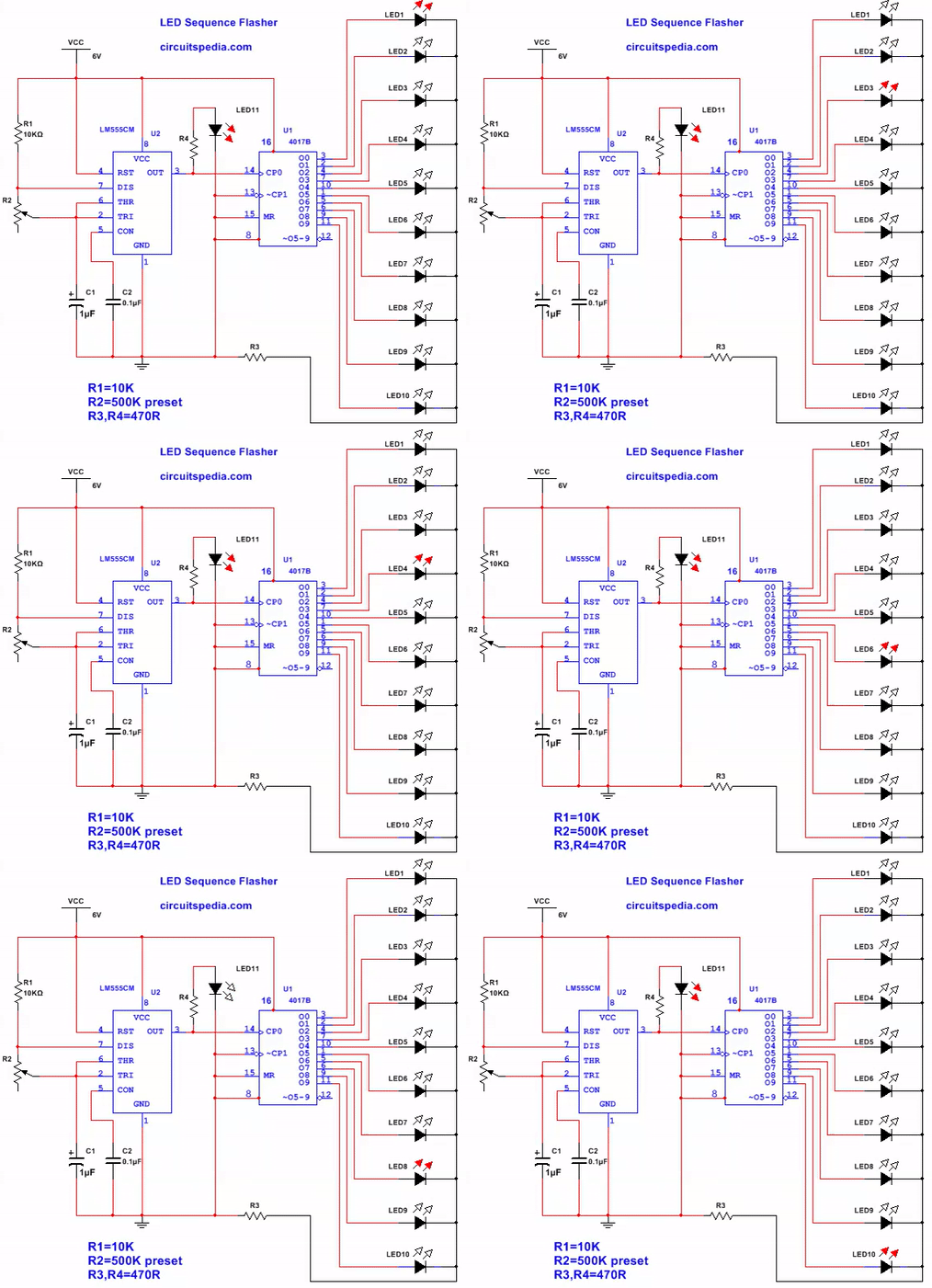
This is the circuit diagram of the LED flasher using 4017. When the clock pulses get at the input pin, all 10 outputs are High (ON) one by one according to the pulse speed at the input pin. At pin 14 Input clock pulse is provided using the 555 timer ic. At each positive clock pulse, the output shift to the next output pin and the previous output is off accordingly. Below animated schematic diagram is showing how it works. This is the simulation of the counter circuit using the led as output detection.
- The supply voltage of this IC is 3V to 15V.
- It is compatible with TTL (Transistor-Transistor Logic).
- The clock speed or operational speed of CD4017 IC is 5 MHz.
Touch on-off Switch using 4017
Operational amplifier (Op-amp)


Hi; I really like your explanation of the CD4017 Decade/Counter. I’m from Canada, and I’m reaaly interested in anything electronics. I’m actually tr4ying to gather informations on a project for my son.He’s building a flying eagle logo sign and want me to install some flashing white leds in sequence. He will need around 100-150 leds. I am thinking of using a 555 timer and some CD4017, and I’m wondering if it is possible to use more than 1 CD4017, since I’ll be using 100-150 leds. Or, is there a simpler way I could do it ??. I would really appreciate if you could give me some advices. Thank you very much.
Maurice Petit